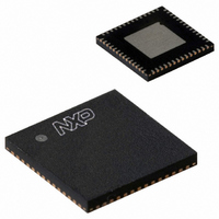
SSTV16859BS,118 NXP Semiconductors, SSTV16859BS,118 Datasheet - Page 8

SSTV16859BS,118
Manufacturer Part Number
SSTV16859BS,118
Description
IC REG BUFFER 26BIT 56HVQFN
Manufacturer
NXP Semiconductors
Series
SSTr
Datasheet
1.SSTV16859BS118.pdf
(14 pages)
Specifications of SSTV16859BS,118
Logic Type
Registered Buffer for DDR
Supply Voltage
2.3 V ~ 2.7 V
Number Of Bits
13, 26
Operating Temperature
0°C ~ 70°C
Mounting Type
Surface Mount
Package / Case
56-VQFN Exposed Pad, 56-HVQFN, 56-SQFN, 56-DHVQFN
Logic Family
SSTV
Logical Function
Registered Buffer
Number Of Elements
1
Number Of Inputs
13
Number Of Outputs
26
High Level Output Current
-20mA
Low Level Output Current
20mA
Propagation Delay Time
2.4ns
Operating Supply Voltage (typ)
2.5V
Operating Supply Voltage (max)
2.7V
Operating Supply Voltage (min)
2.3V
Clock-edge Trigger Type
Posit/Negat-Edge
Polarity
Non-Inverting
Technology
CMOS
Frequency (max)
200(Min)MHz
Mounting
Surface Mount
Pin Count
56
Operating Temp Range
0C to 70C
Operating Temperature Classification
Commercial
Lead Free Status / RoHS Status
Lead free / RoHS Compliant
Other names
935271266118
SSTV16859BS-T
SSTV16859BS-T
SSTV16859BS-T
SSTV16859BS-T
1. This parameter is not necessarily production tested.
2. Data inputs must be below a minimum time of t
3. Data and clock inputs must be held at valid levels (not floating) a minimum time of t
4. For data signal input slew rate
5. For data signal input slew rate
6. CK, CK signals input slew rates are
Philips Semiconductors
TIMING REQUIREMENTS
Over recommended operating conditions; T
NOTES:
SWITCHING CHARACTERISTICS
Over recommended operating conditions; T
Class I, V
2002 Feb 19
SYMBOL
SYMBOL
2.5 V 13-bit to 26-bit SSTL_2
registered buffer for stacked DDR DIMM
f
t
f
t
clock
inact
t
t
max
PHL
t
t
t
t
act
t
t
SL
pd
su
w
h
REF
= V
Clock frequency
Pulse duration, CK, CK HIGH or LOW
Differential inputs active time
Differential inputs inactive time
Setup time, fast slew rate
(see Notes 4 and 6)
Setup time, slow slew rate
(see Notes 5 and 6)
Hold time, fast slew rate
(see Notes 4 and 6)
Hold time, slow slew rate
(see Notes 5 and 6)
Output slew
CK and CK
RESET
TT
= V
DD
0.5 and C
PARAMETER
(INPUT)
(INPUT)
FROM
1 V/ns.
0.5 V/ns and < 1 V/ns.
O
L
= 10 pF (unless otherwise noted) (see Figure 1)
1 V/ns.
amb
amb
= 0 to +70 C (unless otherwise noted) (see Figure 1)
= 0 to +70 C; V
act
max, after RESET is taken high.
DD
= 2.3 – 2.7 V
Data before CK
Data before CK , CK
TEST CONDITIONS
Data after CK
Data after CK , CK
8
(OUTPUT)
(OUTPUT)
Notes 1, 2
Notes 1, 3
TO
Q
Q
O
.
CK
CK
inact
max, after RESET is taken low.
MIN
MIN
200
2.5
1.1
1.1
V
—
—
—
V
1
DD
DD
= 2.5 V 0.2 V
= 2.5 V 0.2 V
LIMITS
LIMITS
0.75
0.75
0.9
0.9
MAX
MAX
200
SSTV16859
2.8
22
22
—
—
6
5
Product data
UNIT
UNIT
MHz
V/ns
MHz
ns
ns
ns
ns
ns
ns
ns
ns
ns


