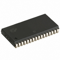
CY7C1019D-10VXI Cypress Semiconductor Corp, CY7C1019D-10VXI Datasheet - Page 7

CY7C1019D-10VXI
Manufacturer Part Number
CY7C1019D-10VXI
Description
IC SRAM 1MBIT 10NS 32SOJ
Manufacturer
Cypress Semiconductor Corp
Type
Asynchronousr
Datasheet
1.CY7C1019D-10ZSXI.pdf
(13 pages)
Specifications of CY7C1019D-10VXI
Memory Size
1M (128K x 8)
Package / Case
32-SOJ
Format - Memory
RAM
Memory Type
SRAM - Asynchronous
Speed
10ns
Interface
Parallel
Voltage - Supply
4.5 V ~ 5.5 V
Operating Temperature
-40°C ~ 85°C
Access Time
10 ns
Supply Voltage (max)
5.5 V
Supply Voltage (min)
4.5 V
Maximum Operating Current
80 mA
Maximum Operating Temperature
+ 85 C
Minimum Operating Temperature
- 40 C
Mounting Style
SMD/SMT
Number Of Ports
1
Operating Supply Voltage
5 V
Memory Configuration
128K X 8
Supply Voltage Range
4.5V To 5.5V
Memory Case Style
SOJ
No. Of Pins
32
Operating Temperature Range
-40°C To +85°C
Rohs Compliant
Yes
Density
1Mb
Access Time (max)
10ns
Sync/async
Asynchronous
Architecture
Not Required
Clock Freq (max)
Not RequiredMHz
Operating Supply Voltage (typ)
5V
Address Bus
17b
Package Type
SOJ
Operating Temp Range
-40C to 85C
Supply Current
80mA
Operating Supply Voltage (min)
4.5V
Operating Supply Voltage (max)
5.5V
Operating Temperature Classification
Industrial
Mounting
Surface Mount
Pin Count
32
Word Size
8b
Number Of Words
128K
Lead Free Status / RoHS Status
Lead free / RoHS Compliant
Lead Free Status / RoHS Status
Lead free / RoHS Compliant, Lead free / RoHS Compliant
Other names
428-1964-5
CY7C1019D-10VXI
CY7C1019D-10VXI
Available stocks
Company
Part Number
Manufacturer
Quantity
Price
Company:
Part Number:
CY7C1019D-10VXI
Manufacturer:
AD
Quantity:
1 760
Part Number:
CY7C1019D-10VXI
Manufacturer:
CYPRESS/赛普拉斯
Quantity:
20 000
Part Number:
CY7C1019D-10VXIT
Manufacturer:
CYPRESS/赛普拉斯
Quantity:
20 000
Switching Waveforms
Write Cycle No. 1 (CE Controlled)
Write Cycle No. 2 (WE Controlled, OE HIGH During Write)
Notes
Document #: 38-05464 Rev. *F
16. Data IO is high impedance if OE = V
17. If CE goes HIGH simultaneously with WE going HIGH, the output remains in a high-impedance state.
18. During this period the IOs are in the output state and input signals should not be applied.
ADDRESS
ADDRESS
DATA IO
DATA IO
WE
WE
CE
OE
CE
NOTE 18
(continued)
IH
t
SA
.
t
HZOE
[16, 17]
t
SA
t
AW
t
AW
t
SCE
t
[16, 17]
t
WC
WC
t
PWE
DATA
t
t
PWE
SD
DATA VALID
t
SCE
IN
t
t
SD
SCE
VALID
t
HD
t
HA
t
HA
t
HD
CY7C1019D
Page 7 of 13
[+] Feedback


