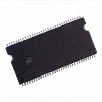
MT46V256M4TG-75:A Micron Technology Inc, MT46V256M4TG-75:A Datasheet - Page 50

MT46V256M4TG-75:A
Manufacturer Part Number
MT46V256M4TG-75:A
Description
IC DDR SDRAM 1GBIT 7.5NS 66TSOP
Manufacturer
Micron Technology Inc
Datasheet
1.MT46V256M4P-6TA_TR.pdf
(82 pages)
Specifications of MT46V256M4TG-75:A
Format - Memory
RAM
Memory Type
DDR SDRAM
Memory Size
1G (256M x 4)
Speed
7.5ns
Interface
Parallel
Voltage - Supply
2.3 V ~ 2.7 V
Operating Temperature
0°C ~ 70°C
Package / Case
66-TSOP
Lead Free Status / RoHS Status
Contains lead / RoHS non-compliant
Figure 23:
ACTIVE
PDF: 09005aef80a2f898/Source: 09005aef82a95a3a
DDR_x4x8x16_Core2.fm - 1Gb DDR: Rev. I, Core DDR: Rev. B 12/07 EN
Extended Mode Register Definition
Notes:
1. n is the most significant row address bit from Table 2 on page 2.
2. The reduced drive strength option is available only on the x16 version. The reduced drive
3. The QFC# option is not supported.
After a row is opened with an ACTIVE command, a READ or WRITE command may be
issued to that row, subject to the
the clock period and rounded up to the next whole number to determine the earliest
clock edge after the ACTIVE command on which a READ or WRITE command can be
entered. For example, a
results in 2.7 clocks rounded to 3. This is reflected in Figure 24 on page 51, which covers
any case where 2 <
same procedure is used to convert other specification limits from time units to clock
cycles).
A row remains active (or open) for accesses until a PRECHARGE command is issued to
that bank. A PRECHARGE command must be issued before opening a different row in
the same bank.
A subsequent ACTIVE command to a different row in the same bank can only be issued
after the previous active row has been “closed” (precharged). The minimum time
interval between successive ACTIVE commands to the same bank is defined by
A subsequent ACTIVE command to another bank can be issued while the first bank is
being accessed, which results in a reduction of total row-access overhead. The minimum
time interval between successive ACTIVE commands to different banks is defined by
t
RRD.
Mn + 2
strength option is not supported on the x4 and x8 versions; contact Micron for future sup-
port of this feature.
0
0
1
1
Mn + 1
En
0
–
0
1
0
1
. . .
0
–
n + 2
Mode Register Definition
Base mode register
Extended mode register
Reserved
Reserved
BA1
E9
0
0
–
E8
n + 1
0
–
t
BA0
RCD (MIN)/
1
E7
0
–
n 1
An
t
E6
RCD specification of 20ns with a 133 MHz clock (7.5ns period)
0
–
. . .
. . .
Operating Mode
E5
0
–
9
50
A9
E4
0
–
t
8
A8
CK ≤ 3 (Figure 24 also shows the same case for
t
RCD specification.
E3
0
–
7
A7 A6 A5 A4 A3
E2
6
0
–
3
Micron Technology, Inc., reserves the right to change products or specifications without notice.
E1
5
0
1
E1, E0
2
Valid
–
4
Drive Strength
3
Reduced
Normal
E0
Operating Mode
0
1
2
A2 A1 A0
1Gb: x4, x8, x16 DDR SDRAM
DS
Reserved
Reserved
1
t
DLL
RCD (MIN) should be divided by
0
Disable
Enable
DLL
Address bus
Extended mode
register (Ex)
©2003 Micron Technology, Inc. All rights reserved.
Operations
t
RRD; the
t
RC.


