IDT70121S55J IDT, Integrated Device Technology Inc, IDT70121S55J Datasheet - Page 8
IDT70121S55J
Manufacturer Part Number
IDT70121S55J
Description
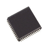
IC SRAM 18KBIT 55NS 52PLCC
Manufacturer
IDT, Integrated Device Technology Inc
Datasheet
1.IDT70121S55J8.pdf
(15 pages)
Specifications of IDT70121S55J
Format - Memory
RAM
Memory Type
SRAM - Dual Port, Asynchronous
Memory Size
18K (2K x 9)
Speed
55ns
Interface
Parallel
Voltage - Supply
4.5 V ~ 5.5 V
Operating Temperature
0°C ~ 70°C
Package / Case
52-PLCC
Density
18Kb
Access Time (max)
55ns
Sync/async
Asynchronous
Architecture
Not Required
Clock Freq (max)
Not RequiredMHz
Operating Supply Voltage (typ)
5V
Address Bus
22b
Package Type
PLCC
Operating Temp Range
0C to 70C
Number Of Ports
2
Supply Current
240mA
Operating Supply Voltage (min)
4.5V
Operating Supply Voltage (max)
5.5V
Operating Temperature Classification
Commercial
Mounting
Surface Mount
Pin Count
52
Word Size
9b
Number Of Words
2K
Lead Free Status / RoHS Status
Contains lead / RoHS non-compliant
Other names
70121S55J
Available stocks
Company
Part Number
Manufacturer
Quantity
Price
Company:

Part Number:
IDT70121S55J
Manufacturer:
IDT
Quantity:
3 000
Company:
Part Number:
IDT70121S55J
Manufacturer:
IDT
Quantity:
8 831
Company:
Part Number:
IDT70121S55J
Manufacturer:
IDT, Integrated Device Technology Inc
Quantity:
10 000
Company:
Part Number:
IDT70121S55J8
Manufacturer:
IDT, Integrated Device Technology Inc
Quantity:
10 000


AC Electrical Characteristics Over the
Operating Temperature and Supply Voltage Range
NOTES:
1. Transition is measured 0mV from Low or High-impedance voltage with Output Test Load (Figure 2).
2. This parameter guaranteed by device characterization, but is not production tested.
3. For MASTER/SLAVE combination, t
4. 'X' in part numbers indicates power rating (S or L).
5. The specified t
6. If OE is LOW during a R/W controlled write cycle, the write pulse width must be the larger of t
WRITE CYCLE
t
t
t
t
t
t
t
t
t
t
t
WRITE CYCLE
t
t
t
t
t
t
t
t
t
t
t
WC
EW
AW
AS
WP
WR
DW
HZ
DH
WZ
OW
WC
EW
AW
AS
WP
WR
DW
HZ
DH
WZ
OW
IDT70121/IDT70125
High-Speed 2K x 9 Dual-Port Static RAM with Busy & Interrupt
Although t
placed on the bus for the required t
as the specified t
Symbol
Symbol
DH
and t
Chip Enable to End-of-Write
Data Valid to End-of-Write
Output High-Z Time
Data Hold Time
Output Active from End-of-Write
Chip Enable to End-of-Write
Data Valid to End-of-Write
Output High-Z Time
Data Hold Time
Output Active from End-of-Write
Write Cycle Time
Address Valid to End-of-Write
Address Set-up Time
Write Pulse Width
Write Recovery Time
Write Enable to Output in High-Z
Write Cycle Time
Address Valid to End-of-Write
Address Set-up Time
Write Pulse Width
Write Recovery Time
Write Enable to Output in High-Z
DH
WP
OW
must be met by the device supplying write date to the RAM under all operating conditions.
.
values will vary over voltage and temperature. The actual t
(5)
(5)
(4)
(4)
(6)
(6)
(1,2,3)
(1,2,3)
WC
DW
. If OE is HIGH during a R/W controlled write cycle, this requirement does not apply and the write pulse can be as short
= t
BAA
+ t
(1,2,3,5)
(1,2,3,5)
(1,3)
(1,3)
WP,
since R/W = V
Parameter
Parameter
IL
must occur after t
6.42
8
DH
will always be smaller than the actual t
BAA
.
WP
or (t
Industrial and Commercial Temperature Ranges
WZ
+ t
DW
Min.
Min.
____
____
____
____
25
20
20
20
12
45
35
35
35
20
(4)
0
0
0
0
0
0
0
0
Com'l Only
Com'l Only
) to allow the I/O drivers to turn off data to be
70121X25
70125X25
70121X45
70125X45
Max.
Max.
____
____
____
____
____
____
____
____
____
____
____
____
____
____
____
____
____
____
20
20
10
10
OW.
Min.
Min.
____
____
____
____
35
30
30
30
20
55
40
40
40
20
0
0
0
0
0
0
0
0
Com'l Only
70121X35
70125X35
70121X55
70125X55
Com'l
& Ind
Max.
Max.
____
____
____
____
____
____
____
____
____
____
____
____
____
____
____
____
____
____
30
30
15
15
2654 tbl 10b
2654 tbl 10a
Unit
Unit
ns
ns
ns
ns
ns
ns
ns
ns
ns
ns
ns
ns
ns
ns
ns
ns
ns
ns
ns
ns
ns
ns
Related parts for IDT70121S55J
Image
Part Number
Description
Manufacturer
Datasheet
Request
R

Part Number:
Description:
TRANSLATION DEVICE DPI 80-PQFP
Manufacturer:
IDT, Integrated Device Technology Inc
Datasheet:
Part Number:
Description:
IDT PART
Manufacturer:
IDT, Integrated Device Technology Inc
Datasheet:
Part Number:
Description:
IC LIU T1/E1/J1 OCTAL 256PBGA
Manufacturer:
IDT, Integrated Device Technology Inc
Datasheet:

Part Number:
Description:
IC FREQ TIMING GENERATOR 28TSSOP
Manufacturer:
IDT, Integrated Device Technology Inc
Datasheet:
Part Number:
Description:
IC CLK DVR PLL 1:10 40VFQFPN
Manufacturer:
IDT, Integrated Device Technology Inc
Datasheet:
Part Number:
Description:
IC CLK FANOUT BUFFER 1:18 32LQFP
Manufacturer:
IDT, Integrated Device Technology Inc
Datasheet:
Part Number:
Description:
IC CLK FANOUT BUFFER 1:18 32LQFP
Manufacturer:
IDT, Integrated Device Technology Inc
Datasheet:
Part Number:
Description:
IC CK505 VREG/RES 56TSSOP
Manufacturer:
IDT, Integrated Device Technology Inc
Datasheet:

Part Number:
Description:
IC SDRAM CLK DVR 1:10 48-TSSOP
Manufacturer:
IDT, Integrated Device Technology Inc
Datasheet:

Part Number:
Description:
IC CLK DVR PLL 1:10 48TSSOP
Manufacturer:
IDT, Integrated Device Technology Inc
Datasheet:
Part Number:
Description:
IC FLEXPC CLK PROGR P4 56-TSSOP
Manufacturer:
IDT, Integrated Device Technology Inc
Datasheet:
Part Number:
Description:
IC FLEXPC CLK PROGR P4 56-TSSOP
Manufacturer:
IDT, Integrated Device Technology Inc
Datasheet:
Part Number:
Description:
IC FLEXPC CLK PROGR P4 56-SSOP
Manufacturer:
IDT, Integrated Device Technology Inc
Datasheet:

Part Number:
Description:
IC PLL CLK DRIVER 2.5V 28-TSSOP
Manufacturer:
IDT, Integrated Device Technology Inc
Datasheet:
Part Number:
Description:
IC CLOCK DRIVER 2.5V 24-TSSOP
Manufacturer:
IDT, Integrated Device Technology Inc
Datasheet: