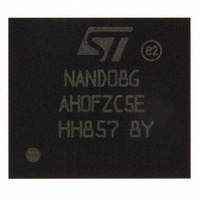
NAND08GAH0FZC5E NUMONYX, NAND08GAH0FZC5E Datasheet - Page 13

NAND08GAH0FZC5E
Manufacturer Part Number
NAND08GAH0FZC5E
Description
IC FLASH 8GBIT 52MHZ 153LFBGA
Manufacturer
NUMONYX
Datasheet
1.NAND02GAH0LZC5E.pdf
(33 pages)
Specifications of NAND08GAH0FZC5E
Format - Memory
FLASH
Memory Type
FLASH - Nand
Memory Size
8G (1G x 8)
Speed
52MHz
Interface
MMC, SPI
Voltage - Supply
3.135 V ~ 3.465 V
Operating Temperature
-25°C ~ 85°C
Package / Case
153-LFBGA
Lead Free Status / RoHS Status
Lead free / RoHS Compliant
Available stocks
Company
Part Number
Manufacturer
Quantity
Price
Company:
Part Number:
NAND08GAH0FZC5E
Manufacturer:
Micron Technology Inc
Quantity:
10 000
NAND02GRH0L, NAND02GAH0L, NAND08GAH0N
5
5.1
5.1.1
5.1.2
5.1.3
5.1.4
5.1.5
MultiMediaCard interface
The signal/pin assignments are listed in
Signals description
Clock (CLK)
The Clock input, CLK, is used to synchronize the memory to the host during command and
data transfers. Each clock cycle gates one bit on the command and on all the data lines. The
Clock frequency, f
Command (CMD)
The CMD signal is a bidirectional command channel used for device initialization and
command transfer. The CMD signal has two operating modes: open-drain and push-pull.
The open-drain mode is used for initialization, while the push-pull mode is used for fast
command transfer. Commands are sent by the MultiMediaCard bus master (or host) to the
device who responds by sending back responses.
Input/outputs (DAT0-DAT7)
DAT0 to DAT7 are bidirectional data channels. The signals operate in push-pull mode. The
NANDxxxxH0x includes internal pull ups for all data lines. These signals cannot be driven
simultaneously by the host and the NANDxxxxH0x device. Right after entering the 4-bit
mode, the card disconnects the internal pull ups of lines DAT1 and DAT2. Correspondingly
right after entering the 8-bit mode, the card disconnects the internal pull ups of lines DAT1,
DAT2 and DAT4-DAT7.
By default, after power-up or hardware reset, only DAT0 is used for data transfers. The host
can configure the device to use a wider data bus, DAT0, DAT0-DAT3 or DAT0-DAT7, for data
transfer.
V
V
power supply for all operations (read, program and erase). The core voltage (V
either within 1.7 V and 1.95 V (NAND02GRH0L) or 2.7 V and 3.6 V (NAND02GAH0L and
NAND08GAH0N).
V
Ground, V
ground.
CC
CC
SS
provides the power supply to the internal core of the memory device. It is the main
ground
core supply voltage
SS,
is the reference for the power supply. It must be connected to the system
PP
, may vary between zero and the maximum clock frequency.
Table
5.
MultiMediaCard interface
CC
) can be
13/33


