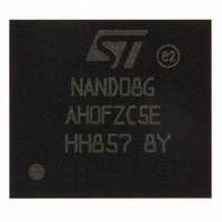
NAND08GAH0FZC5E NUMONYX, NAND08GAH0FZC5E Datasheet - Page 18

NAND08GAH0FZC5E
Manufacturer Part Number
NAND08GAH0FZC5E
Description
IC FLASH 8GBIT 52MHZ 153LFBGA
Manufacturer
NUMONYX
Datasheet
1.NAND02GAH0LZC5E.pdf
(33 pages)
Specifications of NAND08GAH0FZC5E
Format - Memory
FLASH
Memory Type
FLASH - Nand
Memory Size
8G (1G x 8)
Speed
52MHz
Interface
MMC, SPI
Voltage - Supply
3.135 V ~ 3.465 V
Operating Temperature
-25°C ~ 85°C
Package / Case
153-LFBGA
Lead Free Status / RoHS Status
Lead free / RoHS Compliant
Available stocks
Company
Part Number
Manufacturer
Quantity
Price
Company:
Part Number:
NAND08GAH0FZC5E
Manufacturer:
Micron Technology Inc
Quantity:
10 000
High speed MultiMediaCard operation
6
6.1
6.2
6.3
6.4
6.5
18/33
High speed MultiMediaCard operation
All communication between the host and the device is controlled by the host (master).
The following section provides an overview of the identification and data transfer modes,
commands, dependencies, various operation modes and restrictions for controlling the clock
signal. For detailed information, refer to section 7 of the JEDEC Standard Specification No.
JESD84-A43.
Boot mode
The host can read boot data from NANDxxxxH0x by keeping CMD line Low after power-on
or sending CMD0 with argument + 0xFFFFFFFA (optional for slave), before issuing CMD1.
The data can be read from either boot area or user area depending on the register setting.
Refer to section 7.2 of the JEDEC Standard Specification No. JESD84-A43.
Identification mode
When in card identification mode, the host resets the NANDxxxxH0x, validates the operating
voltage range and the access mode, identifies the device and assigns a relative address
(RCA) to it. For more information see section 7.3 of the JEDEC Standard Specification No.
JESD84-A43.
Data transfer mode
The device enters data transfer mode once an RCA is assigned to it. When the device is in
standby mode, issuing the CMD7 command along with the RCA, selects the device and puts
it into the transfer state. The host enters data transfer mode after identifying the
NANDxxxxH0x on the bus. When the device is in standby state, communication over the
CMD and DAT lines is in push-pull mode.
The section 7.5 of the JEDEC Standard Specification No. JESD84-A43 contains more
detailed information about data read and write, erase, write protect management,
lock/unlock operations, the switch function command, high speed mode selection, and bus
testing procedure. Moreover section 7.5.7 contains a detailed description of the reliable
write features supported by the NANDxxxxH0x.
Clock control
Refer to section 7.6 of the JEDEC Standard Specification No. JESD84-A43.
Error conditions
Refer to section 7.7 of the JEDEC Standard Specification No. JESD84-A43.
NAND02GRH0L, NAND02GAH0L, NAND08GAH0N


