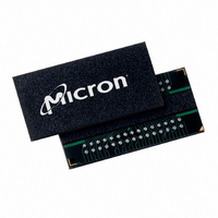
MT46V16M16FG-75:F Micron Technology Inc, MT46V16M16FG-75:F Datasheet - Page 23

MT46V16M16FG-75:F
Manufacturer Part Number
MT46V16M16FG-75:F
Description
IC DDR SDRAM 256MBIT 60FBGA
Manufacturer
Micron Technology Inc
Type
DDR SDRAMr
Datasheet
1.MT46V16M16CY-5BK_TR.pdf
(93 pages)
Specifications of MT46V16M16FG-75:F
Format - Memory
RAM
Memory Type
DDR SDRAM
Memory Size
256M (16Mx16)
Speed
7.5ns
Interface
Parallel
Voltage - Supply
2.3 V ~ 2.7 V
Operating Temperature
0°C ~ 70°C
Package / Case
60-FBGA
Organization
16Mx16
Density
256Mb
Address Bus
15b
Access Time (max)
750ps
Maximum Clock Rate
266MHz
Operating Supply Voltage (typ)
2.5V
Package Type
FBGA
Operating Temp Range
0C to 70C
Operating Supply Voltage (max)
2.7V
Operating Supply Voltage (min)
2.3V
Supply Current
185mA
Pin Count
60
Mounting
Surface Mount
Operating Temperature Classification
Commercial
Lead Free Status / RoHS Status
Contains lead / RoHS non-compliant
Available stocks
Company
Part Number
Manufacturer
Quantity
Price
Company:
Part Number:
MT46V16M16FG-75:F
Manufacturer:
NS
Quantity:
333
Company:
Part Number:
MT46V16M16FG-75:F
Manufacturer:
Micron Technology Inc
Quantity:
10 000
Part Number:
MT46V16M16FG-75:F
Manufacturer:
MICRON
Quantity:
20 000
Company:
Part Number:
MT46V16M16FG-75:F TR
Manufacturer:
Micron Technology Inc
Quantity:
10 000
Table 13:
Figure 11:
PDF: 09005aef80768abb/Source: 09005aef82a95a3a
DDR_x4x8x16_Core2.fm - 256Mb DDR: Rev. O, Core DDR: Rev. B 1/09 EN
Parameter/Condition
Clock input mid-point voltage: CK and CK#
Clock input voltage level: CK and CK#
Clock input differential voltage: CK and CK#
Clock input differential voltage: CK and CK#
Clock input crossing point voltage: CK and CK#
–0.30V
2.80V
1.45V
1.25V
1.05V
CK#
CK
Clock Input Operating Conditions
Notes: 1–5, 16, 17, 31 apply to the entire table; Notes appear on page 35;
0°C ≤ T
SSTL_2 Clock Input
X X
Notes:
A
≤ +70°C; V
1.
2.
3. CK and CK# must cross in this region.
4.
5. CK and CK# must have a minimum 700mV peak-to-peak swing.
6. For AC operation, all DC clock requirements must also be satisfied.
7. Numbers in diagram reflect nominal values for all devices other than -5B.
CK or CK# may not be more positive than V
This provides a minimum of 1.15V to a maximum of 1.35V and is always half of V
CK and CK# must meet at least V
DD
Q = +2.5V ±0.2V, V
Symbol
V
DD
V
V
V
V
MP
IN
ID
ID
IX
= +2.5V ±0.2V (V
(
(
(
(
(
AC
DC
DC
AC
DC
)
)
)
)
21
)
X X
ID
(
DC
0.5 × V
)
MIN when static and is centered around V
Micron Technology, Inc., reserves the right to change products or specifications without notice.
Min
1.15
0.36
–0.3
0.7
DD
Electrical Specifications – DC and AC
DD
DD
Q - 0.2
Q + 0.3V or more negative than V
Q = +2.6V ±0.1V, V
256Mb: x4, x8, x16 DDR SDRAM
0.5 × V
V
V
V
DD
DD
DD
Max
1.35
V
Q + 0.3
Q + 0.6
Q + 0.6
DD
Maximum clock level
MP
Minimum clock level 1
Q + 0.2
(
DC
DD
©2003 Micron Technology, Inc. All rights reserved.
)
2 V
= +2.6V ±0.1V for -5B)
IX
(
AC
Units
)
3
V
V
V
V
V
SS
DD
MP
V
- 0.3V.
1
ID
Q.
(
(
DC
DC
)
)
Notes
V
.
4
7, 10
ID
7, 9
10
7
9
(
AC
) 5


