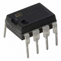
VIPER53DIP-E STMicroelectronics, VIPER53DIP-E Datasheet - Page 12

VIPER53DIP-E
Manufacturer Part Number
VIPER53DIP-E
Description
IC OFFLINE SWIT PWM CM OTP 8DIP
Manufacturer
STMicroelectronics
Series
VIPER™r
Type
Pulse Width Modulator Controllerr
Datasheets
1.VIPER53SPTR-E.pdf
(36 pages)
2.VIPER53DIP-E.pdf
(7 pages)
3.VIPER53DIP-E.pdf
(24 pages)
Specifications of VIPER53DIP-E
Output Isolation
Isolated
Frequency Range
93 ~ 300kHz
Voltage - Input
8.4 ~ 19 V
Voltage - Output
620V
Power (watts)
30W
Operating Temperature
25°C ~ 125°C
Package / Case
8-DIP (0.300", 7.62mm)
Current, Supply
9 mA
Frequency, Oscillator
100 kHz
Package Type
DIP-8
Regulator Type
Switching
Resistance, Thermal, Junction To Case
20 °C/W
Temperature, Operating, Range
-40 to +150 °C
Time, Fall
100 ns
Time, Rise
50 ns
Voltage, Supply
13 V
Power Switch Family
VIPer53DIP
Input Voltage
0 to 19V
Power Switch On Resistance
900mOhm
Output Current
1.6A
Number Of Outputs
Single
Mounting
Through Hole
Supply Current
9mA
Operating Temperature (min)
-40C
Operating Temperature (max)
150C
Operating Temperature Classification
Automotive
Pin Count
8
Mounting Style
Through Hole
For Use With
497-8435 - BOARD EVAL FOR VIPER53 28W497-6458 - BOARD EVAL BASED ON VIPER53-E497-6262 - BOARD REF SGL VIPER53 90-264VAC497-5866 - EVAL BOARD 24W NEG OUT VIPER53E
Lead Free Status / RoHS Status
Lead free / RoHS Compliant
Other names
497-6171-5
VIPer53DIP / VIPer53SP
Figure 14: Off Line Power Supply With Auxiliary Supply Feedback
PRIMARY REGULATION CONFIGURATION
EXAMPLE
The schematic on figure 14 delivers a fixed output
voltage by using the internal error amplifier of the
device in a primary feedback configuration. The
primary auxiliary winding provides a voltage to the
VDD pin, and is automatically regulated at 15 V
thanks to the internal error amplifier connected on
this pin. The secondary voltage has to be adjusted
through the turn ratio of the transformer between
auxiliary and secondary.
The
transconductance one: its output is a current
proportional to the difference of voltage between
the VDD pin and the internal trimmed 15 V
reference,
transconductance value is set at a relatively low
value to control the overall loop gain and insure
stability, this current has to be integrated by a
capacitor (C7 in the above schematic). When the
steady state operation is reached, this capacitor
blocks any DC current from the COMP pin and
imposes a nil error voltage. Therefore, the V
voltage is accurately regulated to 15 V.
12/24
error
AC IN
i.e.
amplifier
F1
R1
the
C1
C4
error
of
R3
C5
the
OSC
T1
VIPer73
voltage.
U1
15V
VIPer53
TOVL
VDD
R6
1k
C6
As
D1
COMP
10nF
C11
R4
is
the
DD
SOURCE
R5
a
C7
C2
DRAIN
This results in a good load regulation, which
depends only on transformer coupling and output
diodes impedance. The current mode structure
takes care of all incoming voltage changes, thus
providing at the same time an excellent line
regulation.
The switching frequency can be set to any value
through the choice of R3 and C5. This allows to
optimize the efficiency of the converter by adopting
the best compromise between switching losses,
EMI (Lower with low switching frequencies) and
transformer size (Smaller with high switching
frequencies). For an output power of a few watts,
typical switching frequencies are comprised
between 20 kHz and 40 kHz because of the small
size of the transformer. For higher power, 70 kHz
to 130 kHz are generally chosen.
The value of the compensation resistor R5 sets the
dynamic behavior of the converter. It can be
adjusted to provide the best compromise between
stability and recovering time with fast load
changes.
C3
D2
D3
R2
T2
D4
C10
C8
L1
C9
DC OUT


