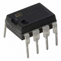
VIPER53DIP-E STMicroelectronics, VIPER53DIP-E Datasheet - Page 17

VIPER53DIP-E
Manufacturer Part Number
VIPER53DIP-E
Description
IC OFFLINE SWIT PWM CM OTP 8DIP
Manufacturer
STMicroelectronics
Series
VIPER™r
Type
Pulse Width Modulator Controllerr
Datasheets
1.VIPER53SPTR-E.pdf
(36 pages)
2.VIPER53DIP-E.pdf
(7 pages)
3.VIPER53DIP-E.pdf
(24 pages)
Specifications of VIPER53DIP-E
Output Isolation
Isolated
Frequency Range
93 ~ 300kHz
Voltage - Input
8.4 ~ 19 V
Voltage - Output
620V
Power (watts)
30W
Operating Temperature
25°C ~ 125°C
Package / Case
8-DIP (0.300", 7.62mm)
Current, Supply
9 mA
Frequency, Oscillator
100 kHz
Package Type
DIP-8
Regulator Type
Switching
Resistance, Thermal, Junction To Case
20 °C/W
Temperature, Operating, Range
-40 to +150 °C
Time, Fall
100 ns
Time, Rise
50 ns
Voltage, Supply
13 V
Power Switch Family
VIPer53DIP
Input Voltage
0 to 19V
Power Switch On Resistance
900mOhm
Output Current
1.6A
Number Of Outputs
Single
Mounting
Through Hole
Supply Current
9mA
Operating Temperature (min)
-40C
Operating Temperature (max)
150C
Operating Temperature Classification
Automotive
Pin Count
8
Mounting Style
Through Hole
For Use With
497-8435 - BOARD EVAL FOR VIPER53 28W497-6458 - BOARD EVAL BASED ON VIPER53-E497-6262 - BOARD REF SGL VIPER53 90-264VAC497-5866 - EVAL BOARD 24W NEG OUT VIPER53E
Lead Free Status / RoHS Status
Lead free / RoHS Compliant
Other names
497-6171-5
introducing a zero and ensuring a correct phase
margin. This configuration is illustrated in figure 18
Figure 19: Typical Transfer Functions
amplifier transfer function for a typical set of values
for C
10 nF (minimum value: 8 nF) should always be
connected to the COMP pin to insure a correct
stability of the internal error amplifier.
The complete converter open loop transfer
function can be built from both power cell and error
amplifier transfer functions. A theoretical example
can be seen in figure 20 for a discontinuous mode
flyback loaded by a simple resistor, regulated from
primary side (no optocoupler, the internal error
amplifier is fully used for regulation). A typical
schematic corresponding to this situation can be
seen on figure 14.
COMP
and R
COMP
Gain (dB)
Phase (°)
-100
-10
. Note that a capacitor of
-10
-20
-30
-40
-50
-60
-70
-80
-90
60
50
40
30
20
10
0
0
1
1
10
10
100
100
Frequency (Hz)
Frequency (Hz)
1k
1k
for the schematic and figure 19 for the error
The transfer function of the power cell is
represented as G(s) in figure 20. It exhibits a pole
which depends on the output load and on the
output capacitor value. As the load of a converter
may change, two curves are shown for two
different values of output resistance value, R
R
appears, due to the output capacitor ESR. Note
that the overall transfer function doesn’t depend on
the input voltage, thanks to the current mode
control.
The error amplifier has a fixed behavior, similar to
the one shown in figure 19. Its bandwidth is limited,
in order to avoid injection of high frequency noise
L2
. A zero at higher frequency values then
10k
10k
100k
100k
Rcomp=4.7k
Ccomp=470nF
Rcomp=4.7k
Ccomp=470nF
VIPer53DIP / VIPer53SP
1M
1M
L1
17/24
and


