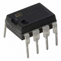
VIPER53DIP-E STMicroelectronics, VIPER53DIP-E Datasheet - Page 2

VIPER53DIP-E
Manufacturer Part Number
VIPER53DIP-E
Description
IC OFFLINE SWIT PWM CM OTP 8DIP
Manufacturer
STMicroelectronics
Series
VIPER™r
Type
Pulse Width Modulator Controllerr
Datasheets
1.VIPER53SPTR-E.pdf
(36 pages)
2.VIPER53DIP-E.pdf
(7 pages)
3.VIPER53DIP-E.pdf
(24 pages)
Specifications of VIPER53DIP-E
Output Isolation
Isolated
Frequency Range
93 ~ 300kHz
Voltage - Input
8.4 ~ 19 V
Voltage - Output
620V
Power (watts)
30W
Operating Temperature
25°C ~ 125°C
Package / Case
8-DIP (0.300", 7.62mm)
Current, Supply
9 mA
Frequency, Oscillator
100 kHz
Package Type
DIP-8
Regulator Type
Switching
Resistance, Thermal, Junction To Case
20 °C/W
Temperature, Operating, Range
-40 to +150 °C
Time, Fall
100 ns
Time, Rise
50 ns
Voltage, Supply
13 V
Power Switch Family
VIPer53DIP
Input Voltage
0 to 19V
Power Switch On Resistance
900mOhm
Output Current
1.6A
Number Of Outputs
Single
Mounting
Through Hole
Supply Current
9mA
Operating Temperature (min)
-40C
Operating Temperature (max)
150C
Operating Temperature Classification
Automotive
Pin Count
8
Mounting Style
Through Hole
For Use With
497-8435 - BOARD EVAL FOR VIPER53 28W497-6458 - BOARD EVAL BASED ON VIPER53-E497-6262 - BOARD REF SGL VIPER53 90-264VAC497-5866 - EVAL BOARD 24W NEG OUT VIPER53E
Lead Free Status / RoHS Status
Lead free / RoHS Compliant
Other names
497-6171-5
VIPer53DIP / VIPer53SP
PIN FUNCTION
CURRENT AND VOLTAGE CONVENTIONS
CONNECTION DIAGRAM
ORDER CODES
2/24
DIP-8
PowerSO-10™
SOURCE
DRAIN
COMP
Name
TOVL
OSC
V
DD
Power supply of the control circuits. Also provides the charging current of the external capacitor during
start-up. The functions of this pin are managed by four threshold voltages:
- V
- V
- V
- V
Power Mosfet source and circuit ground reference.
Power Mosfet drain. Also used by the internal high voltage current source during the start-up phase, for
charging the external V
Input of the current mode structure, and output of the internal error amplifier. Allows the setting of the
dynamic characteristic of the converter through an external passive network. Useful voltage range
extends from 0.5 V to 4.5 V. The Power Mosfet is always off below 0.5 V, and the overload protection is
triggered if the voltage exceeds 4.35V. This action is delayed by the timing capacitor connected to the
TOVL pin.
Allows the connection of an external capacitor for delaying the overload protection, which is triggered by
a voltage on the COMP pin higher than 4.35V.
Allows the setting of the switching frequency through an external Rt-Ct network.
PACKAGE
SOURCE
SOURCE
COMP
DDon
DDoff
DDreg
DDovp
OSC
: Voltage value at which the device stops switching (Typically 8.4 V).
: Voltage value at which the device starts switching (Typically 11.5 V).
1
2
3
4
: Regulation voltage point when working in primary feedback (Trimmed to 15 V).
: Triggering voltage of the overvoltage protection (Trimmed to 18 V).
DIP-8
V
DD
DD
I
DD
8
7
6
5
V
capacitor.
OSC
TOVL
VDD
NC
DRAIN
I
OSC
OSC
V
TOVL
I
15V
TOVL
TOVL
VIPer53DIP
VIPer53SP
VDD
TUBE
V
COMP
Function
I
COMP
COMP
TOVL
DRAIN
VDD
SOURCE
NC
NC
NC
DRAIN
PowerSO-10™
1
2
3
4
5
I
D
V
DS
TAPE and REEL
VIPer53SP13TR
10
9
8
7
6
-
SOURCE
NC
NC
OSC
COMP


