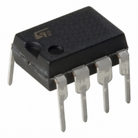
VIPER53DIP-E STMicroelectronics, VIPER53DIP-E Datasheet - Page 5

VIPER53DIP-E
Manufacturer Part Number
VIPER53DIP-E
Description
IC OFFLINE SWIT PWM CM OTP 8DIP
Manufacturer
STMicroelectronics
Series
VIPER™r
Type
Pulse Width Modulator Controllerr
Datasheets
1.VIPER53SPTR-E.pdf
(36 pages)
2.VIPER53DIP-E.pdf
(7 pages)
3.VIPER53DIP-E.pdf
(24 pages)
Specifications of VIPER53DIP-E
Output Isolation
Isolated
Frequency Range
93 ~ 300kHz
Voltage - Input
8.4 ~ 19 V
Voltage - Output
620V
Power (watts)
30W
Operating Temperature
25°C ~ 125°C
Package / Case
8-DIP (0.300", 7.62mm)
Current, Supply
9 mA
Frequency, Oscillator
100 kHz
Package Type
DIP-8
Regulator Type
Switching
Resistance, Thermal, Junction To Case
20 °C/W
Temperature, Operating, Range
-40 to +150 °C
Time, Fall
100 ns
Time, Rise
50 ns
Voltage, Supply
13 V
Power Switch Family
VIPer53DIP
Input Voltage
0 to 19V
Power Switch On Resistance
900mOhm
Output Current
1.6A
Number Of Outputs
Single
Mounting
Through Hole
Supply Current
9mA
Operating Temperature (min)
-40C
Operating Temperature (max)
150C
Operating Temperature Classification
Automotive
Pin Count
8
Mounting Style
Through Hole
For Use With
497-8435 - BOARD EVAL FOR VIPER53 28W497-6458 - BOARD EVAL BASED ON VIPER53-E497-6262 - BOARD REF SGL VIPER53 90-264VAC497-5866 - EVAL BOARD 24W NEG OUT VIPER53E
Lead Free Status / RoHS Status
Lead free / RoHS Compliant
Other names
497-6171-5
ELECTRICAL CHARACTERISTICS (T
SUPPLY SECTION
ERROR AMPLIFIER SECTION
Note 6. In order to insure a correct stability of the error amplifier, a capacitor of 10nF (minimum value: 8nF) should always be present on
Symbol
Symbol
V
V
V
V
I
I
I
V
V
I
I
V
COMPlo
COMPhi
DDchoff
V
V
AV
COMPlo
COMPhi
DDch1
DDch2
G
DSstart
DDhyst
I
I
DDovp
DDreg
G
DD0
DD1
DDoff
DDon
DDreg
BW
OL
m
the COMP pin.
Drain Voltage Starting
Threshold
Startup Charging Current
Startup Charging Current
Startup Charging Current
in Thermal Shutdown
Operating Supply Current
Not Switching
Operating Supply Current
Switching
V
Shutdown Threshold
V
V
Hysteresis
V
Shutdown Threshold
V
V
Total Variation
Unity Gain Bandwidth
Voltage Gain
DC Transconductance
Output Low Level
Output High Level
Output Sinking Current
Output Sourcing Current
DD
DD
DD
DD
DD
DD
Undervoltage
Overvoltage
Startup Threshold
Threshold
Regulation Point
Regulation Point
Parameter
Parameter
V
V
V
V
T
F
F
(See figure 2)
(See figure 2)
(See figure 2)
(See figure 7)
I
I
From Input =V
I
I
V
I
I
V
V
COMP
COMP
COMP
COMP
COMP
COMP
j
sw
sw
DD
DD
DD
DD
COMP
COMP
COMP
> T
j
=0kHz; V
=100kHz
=25°C, V
=5V; I
=0 ... 5V; V
=10V; V
=5V; V
SD
=0mA
=0mA; T
=0mA
=0mA
=-0.4mA; V
=0.4mA; V
=2.5V
=2.5V; V
=2.5V; V
- T
DD
DS
HYST
Test Conditions
Test Conditions
DS
=0mA
COMP
=100V
DD
DD
=100V
j
=0 ... 100°C
DS
DD
DD
DD
DD
=13V, unless otherwise specified)
to Output = V
=100V (See figure 2)
=16V
=14V
=0V
=14V
=16V
(See figure 10)
(See figure 10)
(See figure 2)
(See figure 5)
(See figure 3)
(See figure 3)
(See figure 3)
(See figure 3)
(See note 6)
COMP
Min.
10.2
Min.
14.5
7.5
2.6
17
40
0
1
VIPer53DIP / VIPer53SP
Typ.
Typ.
11.5
-0.6
700
-12
8.4
3.1
1.4
0.2
4.5
0.6
34
18
15
45
-2
8
9
2
Max.
Max.
12.8
15.5
9.3
1.8
50
19
11
Unit
Unit
kHz
mA
mA
mA
mA
mA
mS
mA
mA
dB
%
V
V
V
V
V
V
V
V
5/24


