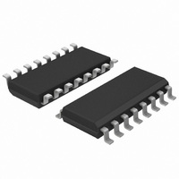
74HC4511D,653 NXP Semiconductors, 74HC4511D,653 Datasheet - Page 2

74HC4511D,653
Manufacturer Part Number
74HC4511D,653
Description
IC LATCH/DECODER/DRIVER 16SOIC
Manufacturer
NXP Semiconductors
Series
74HCr
Datasheet
1.74HC4511D653.pdf
(12 pages)
Specifications of 74HC4511D,653
Package / Case
16-SOIC (3.9mm Width)
Display Type
LED
Configuration
7 Segment
Interface
BCD
Voltage - Supply
2 V ~ 6 V
Operating Temperature
-40°C ~ 125°C
Mounting Type
Surface Mount
Product
Latch/Decoder/Driver
Logic Family
HC
Number Of Lines (input / Output)
4.0 / 7.0
Propagation Delay Time
50 ns
Supply Voltage (max)
6 V
Supply Voltage (min)
2 V
Maximum Operating Temperature
+ 125 C
Minimum Operating Temperature
- 40 C
Mounting Style
SMD/SMT
Number Of Input Lines
4.0
Number Of Output Lines
7.0
Lead Free Status / RoHS Status
Lead free / RoHS Compliant
Current - Supply
-
Digits Or Characters
-
Lead Free Status / Rohs Status
Lead free / RoHS Compliant
Other names
74HC4511D-T
74HC4511D-T
933714880653
74HC4511D-T
933714880653
Available stocks
Company
Part Number
Manufacturer
Quantity
Price
Part Number:
74HC4511D,653
Manufacturer:
NXP/恩智浦
Quantity:
20 000
Philips Semiconductors
FEATURES
GENERAL DESCRIPTION
The 74HC/HCT4511 are high-speed Si-gate CMOS
devices and are pin compatible with “4511” of the “4000B”
series. They are specified in compliance with JEDEC
standard no. 7A.
The 74HC/HCT4511 are BCD to 7-segment
latch/decoder/drivers with four address inputs (D
an active LOW latch enable input (LE), an active LOW
QUICK REFERENCE DATA
GND = 0 V; T
Notes
1. C
2. For HC the condition is V
December 1990
SYMBOL
t
C
C
PHL
Latch storage of BCD inputs
Blanking input
Lamp test input
Driving common cathode LED displays
Guaranteed 10 mA drive capability per output
Output capability: non-standard
I
BCD to 7-segment latch/decoder/driver
I
PD
CC
f
f
C
V
For HCT the condition is V
i
o
/ t
CC
PD
= input frequency in MHz
L
category: MSI
= output frequency in MHz
(C
PLH
= output load capacitance in pF
P
= supply voltage in V
is used to determine the dynamic power dissipation (P
L
D
= C
V
CC
amb
PD
2
= 25 C; t
PARAMETER
propagation delay
input capacitance
power dissipation capacitance per latch
V
f
D
LE to Q
BI to Q
LT to Q
o
CC
) = sum of outputs
n
to Q
2
f
n
r
i
n
n
n
= t
I
I
f
= GND to V
= GND to V
= 6 ns
(C
L
V
CC
2
CC
CC
f
o
) where:
1.5 V
1
to D
4
),
2
CONDITIONS
C
notes 1 and 2
ripple blanking input (BI), an active LOW lamp test input
(LT), and seven active HIGH segment outputs (Q
When LE is LOW, the state of the segment outputs (Q
Q
When LE goes HIGH, the last data present on D
stored in the latches and the segment outputs remain
stable.
When LT is LOW, all the segment outputs are HIGH
independent of all other input conditions. With LT HIGH, a
LOW on BI forces all segment outputs LOW. The inputs LT
and BI do not affect the latch circuit.
APPLICATIONS
L
g
D
Driving LED displays
Driving incandescent displays
Driving fluorescent displays
Driving LCD displays
Driving gas discharge displays
= 15 pF; V
) is determined by the data on D
in W):
CC
= 5 V
24
23
19
12
3.5
64
HC
TYPICAL
74HC/HCT4511
Product specification
24
24
20
13
3.5
64
1
to D
HCT
4
.
ns
ns
ns
ns
pF
pF
1
to D
a
UNIT
to Q
4
a
are
g
to
).


