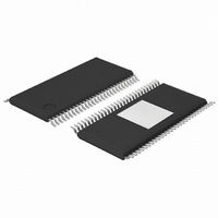
PCF8576CTT/1,118 NXP Semiconductors, PCF8576CTT/1,118 Datasheet - Page 26

PCF8576CTT/1,118
Manufacturer Part Number
PCF8576CTT/1,118
Description
IC LCD DVR UNIVERSAL 56-HTSSOP
Manufacturer
NXP Semiconductors
Datasheet
1.PCF8576CTT1118.pdf
(57 pages)
Specifications of PCF8576CTT/1,118
Package / Case
56-TSSOP Exposed Pad, 56-eTSSOP, 56-HTSSOP
Display Type
LCD
Configuration
40 Segment
Interface
I²C
Current - Supply
120µA
Voltage - Supply
2 V ~ 6 V
Operating Temperature
-40°C ~ 85°C
Mounting Type
Surface Mount
Number Of Digits
20
Number Of Segments
160
Maximum Clock Frequency
315 KHz
Operating Supply Voltage
2 V to 6 V
Maximum Power Dissipation
400 mW
Maximum Supply Current
120 uA
Lead Free Status / RoHS Status
Lead free / RoHS Compliant
Digits Or Characters
-
Lead Free Status / Rohs Status
Lead free / RoHS Compliant
Other names
935284868118
PCF8576CTT/1-T
PCF8576CTT/1-T
PCF8576CTT/1-T
PCF8576CTT/1-T
NXP Semiconductors
PCF8576C
Product data sheet
7.16.5 PCF8576C I
7.16.6 Input filter
7.17 I
The PCF8576C acts as an I
transmit data to an I
the acknowledge signals of the selected devices. Device selection depends on the
I
In single device application, the hardware subaddress inputs A0, A1, and A2 are normally
tied to V
A0, A1, and A2 are tied to V
devices with a common I
In the power-saving mode it is possible that the PCF8576C is not able to keep up with the
highest transmission rates when large amounts of display data are transmitted. If this
situation occurs, the PCF8576C forces the SCL line LOW until its internal operations are
completed. This is known as the clock synchronization feature of the I
to slow down fast transmitters. Data loss does not occur.
To enhance noise immunity in electrically adverse environments, RC low-pass filters are
provided on the SDA and SCL lines.
Two I
The least significant bit of the slave address that a PCF8576C responds to is defined by
the level tied at its input SA0. Therefore, two types of PCF8576C can be distinguished on
the same I
2
2
Fig 18. Acknowledgement of the I
C-bus slave address, the transferred command data and the hardware subaddress.
•
•
C-bus protocol
Up to 16 PCF8576Cs on the same I
The use of two types of LCD multiplex on the same I
2
C-bus slave addresses (0111000 and 0111001) are reserved for the PCF8576C.
by transmitter
SS
data output
by receiver
data output
SCL from
2
which defines the hardware subaddress 0. In multiple device applications
C-bus which allows:
master
2
C-bus controller
All information provided in this document is subject to legal disclaimers.
2
condition
C-bus master receiver. The only data output from the PCF8576C are
START
S
Rev. 10 — 22 July 2010
2
C-bus slave address have the same hardware subaddress.
2
SS
C-bus slave receiver. It does not initiate I
or V
2
1
DD
C-bus
using a binary coding scheme so that no two
2
C-bus for very large LCD applications.
Universal LCD driver for low multiplex rates
2
2
C-bus.
not acknowledge
acknowledge
8
PCF8576C
acknowledgement
clock pulse for
2
2
C-bus and serves
C-bus transfers or
© NXP B.V. 2010. All rights reserved.
9
mbc602
26 of 57


