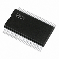
PCF8578T/1,118 NXP Semiconductors, PCF8578T/1,118 Datasheet - Page 27

PCF8578T/1,118
Manufacturer Part Number
PCF8578T/1,118
Description
IC LCD DRIVER ROW/COLUMN 56-VSOP
Manufacturer
NXP Semiconductors
Specifications of PCF8578T/1,118
Package / Case
56-VSOP
Display Type
LCD
Configuration
Dot Matrix
Interface
I²C
Voltage - Supply
2.5 V ~ 6 V
Operating Temperature
-40°C ~ 85°C
Mounting Type
Surface Mount
Number Of Digits
24
Number Of Segments
7
Maximum Clock Frequency
3.3 KHz
Operating Supply Voltage
2.5 V to 6 V
Maximum Power Dissipation
400 mW
Maximum Operating Temperature
+ 150 C
Attached Touch Screen
No
Maximum Supply Current
50 mA
Minimum Operating Temperature
- 65 C
Lead Free Status / RoHS Status
Lead free / RoHS Compliant
Current - Supply
-
Digits Or Characters
-
Lead Free Status / Rohs Status
Details
Other names
935278868118
PCF8578TD-T
PCF8578TD-T
PCF8578TD-T
PCF8578TD-T
Available stocks
Company
Part Number
Manufacturer
Quantity
Price
Part Number:
PCF8578T/1,118
Manufacturer:
NXP/恩智浦
Quantity:
20 000
Philips Semiconductors
12 DC CHARACTERISTICS
V
Notes
1. Outputs are open; inputs at V
2. Resets all logic when V
3. Periodically sampled; not 100% tested.
4. Resistance measured between output terminal (R0 to R7, R8/C8 to R31/C31 and C32 to C39) and bias input
2003 Apr 14
Supplies
V
V
I
I
V
Logic
V
V
I
I
I
I
I
C
LCD outputs
I
V
R
R
DD1
DD2
OL1
OH1
OL2
L1
L2
L3
DD
SYMBOL
DD
LCD
POR
IL
IH
DC
i
ROW
COL
LCD row/column driver for
dot matrix graphic displays
(V
(see Table 2):
a) V
b) Row mode, R0 to R7 and R8/C8 to R31/C31: V
c) Column mode, R8/C8 to R31/C31 and C32 to C39: V
= 2.5 to 6 V; V
2
to V
op
= V
5
, V
supply voltage
LCD supply voltage
supply current external clock
supply current internal clock
power-on reset level
LOW level input voltage
HIGH level input voltage
LOW level output current at SYNC
and CLK
HIGH level output current at SYNC
and CLK
LOW level output current at SDA
leakage current at SDA, SCL, SYNC,
CLK, TEST and SA0
leakage current at OSC
input capacitance at SCL and SDA
leakage current at V
DC component of LCD drivers
R0 to R7, R8/C8 to R31/C31 and
C32 to C39
output resistance R0 to R7 and
R8/C8 to R31/C31
output resistance R8/C8 to R31/C31
and C32 to C39
DD
DD
and V
SS
V
LCD
= 0 V; V
LCD
PARAMETER
= 9 V.
DD
) when the specified current flows through one output under the following conditions
LCD
< V
DD
= V
POR
2
to V
or V
DD
.
5
SS
3.5 V to V
; I
2
C-bus inactive; external clock with 50% duty factor.
DD
f
R
note 2
V
V
V
V
V
note 3
V
row mode; note 4
column mode; note 4
CLK
OL
OH
OL
i
i
i
OSC
2
= V
= V
= V
= 1 V; V
= 0.4 V; V
9 V; T
= 2 kHz; note 1
CONDITIONS
= 4 V; V
V
27
= 330 k
DD
DD
DD
LCD
3
or V
or V
amb
V
DD
DD
LCD
6.65 V; V
SS
LCD
= 40 to 85 C; unless otherwise specified.
DD
= 5 V
= 5 V
= 5 V
4.70 V; V
5
2.5
V
0.8
V
0.7V
1
3
V
2
DD
SS
LCD
MIN.
4
DD
V
9
2.35 V; I
LCD
6
20
1.3
1.5
3
20
TYP.
4.30 V; I
LOAD
Product specification
6.0
V
15
50
1.8
0.3V
V
5
3
6
= 150 A.
LOAD
1
1
1
2
DD
DD
MAX.
PCF8578
DD
= 100 A.
3.5 V
V
V
V
V
mA
mA
mA
mA
pF
mV
k
k
UNIT
A
A
A
A


