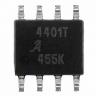
A4401KL-T Allegro Microsystems Inc, A4401KL-T Datasheet - Page 13

A4401KL-T
Manufacturer Part Number
A4401KL-T
Description
IC QUASI FLYBACK CONVERTER 8SOIC
Manufacturer
Allegro Microsystems Inc
Datasheet
1.A4401KLTR-T.pdf
(17 pages)
Specifications of A4401KL-T
Display Type
Vacuum Fluorescent (VF)
Current - Supply
2.3mA
Voltage - Supply
7 V ~ 40 V
Operating Temperature
-40°C ~ 125°C
Mounting Type
Surface Mount
Package / Case
8-SOIC (3.9mm Width)
Lead Free Status / RoHS Status
Lead free / RoHS Compliant
Interface
-
Configuration
-
Digits Or Characters
-
A4401
filtering, it is imperative that the “power loop” formed
by the input filter, primary winding, MOSFET, Q1,
and sense resistor is as short and “tight” as possible.
This means components should be placed as close
together as possible, and the loop area should be
minimized, in order to reduce the effects of magnetic
pickup and noise generation at higher frequencies. A
ground plane is not necessary, however, a good star
ground connection should be formed between the
input filter capacitor and the sense resistor. Circuit
traces should be as wide as possible, in order to mini-
mize leakage inductance. Figure 3 illustrates the main
power loop.
A local ground plane around the A4401 can be used to
minimize ground bounce issues. This can be done with
a simple connection from the ground pin of the A4401
to the star ground, being careful to avoid any connec-
tion between this local ground plane and the power
loop.
The compensation components connected to the
COMP pin, the filter capacitor connected to VIN, the
feedback resistors connected to VA, and the resonant
Figure 4. One of three output power loops
L
SEC
Minimize this loop area
Automotive Quasi-Resonant Flyback Control IC
C
OUT
capacitor connected to LX should be located as close
to their respective pins as possible. In addition, the
length of the traces between those components and
ground should be as short as possible.
Secondary Block
be laid out with identical principles relative to the pri-
mary side power circuit, that is, with each secondary
winding, rectifying diode, and output capacitor posi-
tioned close together and forming a tight loop.
The high voltage output circuits should be kept well
away from all the control circuitry. It is recommended
that good connections be made between each of the
local output grounds and the star ground. In addition,
all of the output grounds should be connected together
via wide traces and not ground planes. Figure 4 illus-
trates one of the output loops.
The feedback resistor connected to the regulated
output rail should be located as close to the VA pin as
possible. The PCB trace that connects the top of this
resistor to the output rail should not be located near
any of the output power loops or ground connections.
Electromagnetic Interference
Some of the previous sections provide information
on reducing EMI in terms of input filter capacitance
selection, magnetics design (to achieve zero voltage
switching at nominal input voltage), and board lay-
out. This section provides some additional advice on
reducing EMI.
Effects of Magnetics Design on 0 V Switching
ure 5 illustrates a converter running at full power with
V
LX and the lower trace is the voltage across the sense
resistor (essentially the current through the primary
winding and the MOSFET, Q1). The magnetic set in
this case was designed to achieve 0 V switching at
a V
BAT
BAT
= 13.5 V. The upper trace is the voltage across
of 7 V.
Each output power circuit should
115 Northeast Cutoff, Box 15036
Allegro MicroSystems, Inc.
Worcester, Massachusetts 01615-0036 (508) 853-5000
www.allegromicro.com
Fig-
13


