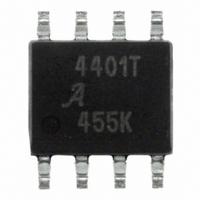
A4401KL-T Allegro Microsystems Inc, A4401KL-T Datasheet - Page 9

A4401KL-T
Manufacturer Part Number
A4401KL-T
Description
IC QUASI FLYBACK CONVERTER 8SOIC
Manufacturer
Allegro Microsystems Inc
Datasheet
1.A4401KLTR-T.pdf
(17 pages)
Specifications of A4401KL-T
Display Type
Vacuum Fluorescent (VF)
Current - Supply
2.3mA
Voltage - Supply
7 V ~ 40 V
Operating Temperature
-40°C ~ 125°C
Mounting Type
Surface Mount
Package / Case
8-SOIC (3.9mm Width)
Lead Free Status / RoHS Status
Lead free / RoHS Compliant
Interface
-
Configuration
-
Digits Or Characters
-
A4401
for more information). The current that flows in and
out of the capacitor is similar to the current that flows
through the corresponding rectifier diode.
Worst case power dissipation due to the ESR will
occur at V
cycle under these conditions is a maximum of 0.7.
The rms current in the capacitor can be found as fol-
lows:
When selecting a suitable capacitor, the rms current
rating should have reasonable margin with respect to
the above value. In addition, the current rating should
be derated to take into account the frequency correc-
tion at values of less than 100 kHz.
The impedance of the output capacitor will affect the
amount of voltage ripple and noise that appears on
the output. The impedance is composed of two com-
ponents: ESR and reactance, X
amount of capacitance on the output, the ESR will
tend to dominate the overall impedance.
The ESR can be estimated by multiplying the capaci-
tance reactance by the dissipation factor, DF (tan δ):
Note that DF is normally quoted at 25°C, however,
it is usually fairly constant as the temperature is
increased.
The peak to peak voltage can then be found:
The voltage rating should be chosen to provide at least
a 20% margin above the maximum output voltage.
Control Loop
As the converter operates in discontinuous mode,
the inductor does not feature in the power stage. The
BAT
ESR =
(min) and maximum load. The duty
V
I
RMS
pk-pk
2 × × f
= 4 × I
= ESR × I
SW
1
LOAD
× C
LOAD
×
Automotive Quasi-Resonant Flyback Control IC
C
OUT
. Even with a modest
⎛
⎜ ⎜
⎝
× 4
0.7
3
× DF
⎞
⎟ ⎟
⎠
½
.
.
.
(16)
(17)
(18)
power stage effectively contains one pole formed by
the output capacitors and loads.
In terms of “closing the loop,” the optimal shaping
components are shown in the Functional Block dia-
gram, connected to the COMP pin. The control loop is
optimized for an equivalent output capacitor of 22 μF.
Larger capacitor values can be used, however, those
will tend to reduce the bandwidth of the control loop.
Smaller values should not be used, as they may cause
instability issues.
Magnetics Design
The following are the known variables:
• Maximum output power, P
• Minimum battery voltage, V
• Minimum switching frequency, f
• Maximum duty cycle. This should typically not
• Efficiency of converter, η% , at V
• Resonant capacitor, C11, connected between the
• Known magnetic core set. Material selection should
occurs at V
is recommended that the lowest possible switching
frequency be used, in order to minimize switching
losses and to shift the differential harmonics down
the frequency spectrum. This is a compromise with
the sizing of the magnetics and filtering components.
exceed 0.7, in order to avoid excessive losses in the
secondary output circuits.
typically be between 80% and 85%.
LX pin and ground. The resonant half period of 1 μs
may be achieved with the parasitic capacitance that
exists in the circuit. Fine tuning can be performed by
adding additional capacitance.
be based on performance at elevated temperature,
and include consideration of flux density, losses,
Curie temperature, and so forth.
BAT
(min) and maximum load. Note, it
115 Northeast Cutoff, Box 15036
Allegro MicroSystems, Inc.
Worcester, Massachusetts 01615-0036 (508) 853-5000
www.allegromicro.com
OUT
BAT
.
(min).
SW
BAT
(min). This
(min). This will
9


