TZA3011BVH/C2,551 NXP Semiconductors, TZA3011BVH/C2,551 Datasheet - Page 25
TZA3011BVH/C2,551
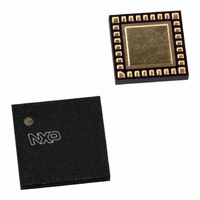
Manufacturer Part Number
TZA3011BVH/C2,551
Description
IC LASER DRIVER 3.2GBPS 32-HBCC
Manufacturer
NXP Semiconductors
Series
A-rate™r
Type
Laser Diode Driver (Fiber Optic)r
Datasheet
1.TZA3011AVHC2557.pdf
(30 pages)
Specifications of TZA3011BVH/C2,551
Data Rate
3.2Gbps
Number Of Channels
1
Voltage - Supply
3.14 V ~ 3.47 V
Current - Supply
40mA
Current - Modulation
100mA
Current - Bias
100mA
Operating Temperature
-40°C ~ 85°C
Package / Case
32-HBCC
Mounting Type
Surface Mount
Lead Free Status / RoHS Status
Lead free / RoHS Compliant
Other names
935269941551
TZA3011BVHW-S
TZA3011BVHW-S
TZA3011BVHW-S
TZA3011BVHW-S


Philips Semiconductors
14. Soldering
9397 750 14437
Product data sheet
14.1 Introduction to soldering surface mount packages
14.2 Reflow soldering
14.3 Wave soldering
This text gives a very brief insight to a complex technology. A more in-depth account of
soldering ICs can be found in our Data Handbook IC26; Integrated Circuit Packages
(document order number 9398 652 90011).
There is no soldering method that is ideal for all surface mount IC packages. Wave
soldering can still be used for certain surface mount ICs, but it is not suitable for fine pitch
SMDs. In these situations reflow soldering is recommended.
Reflow soldering requires solder paste (a suspension of fine solder particles, flux and
binding agent) to be applied to the printed-circuit board by screen printing, stencilling or
pressure-syringe dispensing before package placement. Driven by legislation and
environmental forces the worldwide use of lead-free solder pastes is increasing.
Several methods exist for reflowing; for example, convection or convection/infrared
heating in a conveyor type oven. Throughput times (preheating, soldering and cooling)
vary between 100 seconds and 200 seconds depending on heating method.
Typical reflow peak temperatures range from 215 C to 270 C depending on solder paste
material. The top-surface temperature of the packages should preferably be kept:
Moisture sensitivity precautions, as indicated on packing, must be respected at all times.
Conventional single wave soldering is not recommended for surface mount devices
(SMDs) or printed-circuit boards with a high component density, as solder bridging and
non-wetting can present major problems.
To overcome these problems the double-wave soldering method was specifically
developed.
If wave soldering is used the following conditions must be observed for optimal results:
•
•
•
•
below 225 C (SnPb process) or below 245 C (Pb-free process)
– for all BGA, HTSSON..T and SSOP..T packages
– for packages with a thickness
– for packages with a thickness < 2.5 mm and a volume
below 240 C (SnPb process) or below 260 C (Pb-free process) for packages with a
thickness < 2.5 mm and a volume < 350 mm
Use a double-wave soldering method comprising a turbulent wave with high upward
pressure followed by a smooth laminar wave.
For packages with leads on two sides and a pitch (e):
– larger than or equal to 1.27 mm, the footprint longitudinal axis is preferred to be
thick/large packages.
parallel to the transport direction of the printed-circuit board;
Rev. 06 — 20 January 2005
2.5 mm
30 Mbit/s up to 3.2 Gbit/s A-rate
TZA3011A; TZA3011B
3
so called small/thin packages.
© Koninklijke Philips Electronics N.V. 2005. All rights reserved.
350 mm
3
so called
laser drivers
25 of 30
Related parts for TZA3011BVH/C2,551
Image
Part Number
Description
Manufacturer
Datasheet
Request
R

Part Number:
Description:
IC LASER DRIVER 3.2GBPS 32-HBCC
Manufacturer:
NXP Semiconductors
Datasheet:

Part Number:
Description:
NXP Semiconductors designed the LPC2420/2460 microcontroller around a 16-bit/32-bitARM7TDMI-S CPU core with real-time debug interfaces that include both JTAG andembedded trace
Manufacturer:
NXP Semiconductors
Datasheet:

Part Number:
Description:
NXP Semiconductors designed the LPC2458 microcontroller around a 16-bit/32-bitARM7TDMI-S CPU core with real-time debug interfaces that include both JTAG andembedded trace
Manufacturer:
NXP Semiconductors
Datasheet:
Part Number:
Description:
NXP Semiconductors designed the LPC2468 microcontroller around a 16-bit/32-bitARM7TDMI-S CPU core with real-time debug interfaces that include both JTAG andembedded trace
Manufacturer:
NXP Semiconductors
Datasheet:
Part Number:
Description:
NXP Semiconductors designed the LPC2470 microcontroller, powered by theARM7TDMI-S core, to be a highly integrated microcontroller for a wide range ofapplications that require advanced communications and high quality graphic displays
Manufacturer:
NXP Semiconductors
Datasheet:
Part Number:
Description:
NXP Semiconductors designed the LPC2478 microcontroller, powered by theARM7TDMI-S core, to be a highly integrated microcontroller for a wide range ofapplications that require advanced communications and high quality graphic displays
Manufacturer:
NXP Semiconductors
Datasheet:
Part Number:
Description:
The Philips Semiconductors XA (eXtended Architecture) family of 16-bit single-chip microcontrollers is powerful enough to easily handle the requirements of high performance embedded applications, yet inexpensive enough to compete in the market for hi
Manufacturer:
NXP Semiconductors
Datasheet:
Part Number:
Description:
The XA-S3 device is a member of Philips Semiconductors? XA(eXtended Architecture) family of high performance 16-bitsingle-chip microcontrollers
Manufacturer:
NXP Semiconductors
Datasheet:

Part Number:
Description:
The NXP BlueStreak LH75401/LH75411 family consists of two low-cost 16/32-bit System-on-Chip (SoC) devices
Manufacturer:
NXP Semiconductors
Datasheet:
Part Number:
Description:
The NXP LPC3130/3131 combine an 180 MHz ARM926EJ-S CPU core, high-speed USB2
Manufacturer:
NXP Semiconductors
Datasheet:
Part Number:
Description:
The NXP LPC3141 combine a 270 MHz ARM926EJ-S CPU core, High-speed USB 2
Manufacturer:
NXP Semiconductors
Part Number:
Description:
The NXP LPC3143 combine a 270 MHz ARM926EJ-S CPU core, High-speed USB 2
Manufacturer:
NXP Semiconductors

Part Number:
Description:
The NXP LPC3152 combines an 180 MHz ARM926EJ-S CPU core, High-speed USB 2
Manufacturer:
NXP Semiconductors
Part Number:
Description:
The NXP LPC3154 combines an 180 MHz ARM926EJ-S CPU core, High-speed USB 2
Manufacturer:
NXP Semiconductors