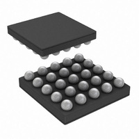
LP5526TL/NOPB National Semiconductor, LP5526TL/NOPB Datasheet - Page 21

LP5526TL/NOPB
Manufacturer Part Number
LP5526TL/NOPB
Description
IC LED DRVR WT/RGB BCKLT 25-USMD
Manufacturer
National Semiconductor
Series
PowerWise®r
Type
Backlight, White LED, RGB (I²C Interface)r
Datasheet
1.LP5526TLNOPB.pdf
(32 pages)
Specifications of LP5526TL/NOPB
Constant Current
Yes
Topology
PWM, Step-Up (Boost)
Number Of Outputs
5
Internal Driver
Yes
Type - Primary
Backlight, Light Management Unit (LMU)
Type - Secondary
RGB, White LED
Frequency
1MHz
Voltage - Supply
3 V ~ 5.5 V
Voltage - Output
8 V ~ 20 V
Mounting Type
Surface Mount
Package / Case
25-MicroSMD
Operating Temperature
-30°C ~ 85°C
Current - Output / Channel
150mA
Internal Switch(s)
Yes
Efficiency
88%
For Use With
LP5526TLEV - BOARD EVAL LP5526 LMU LED DRIVER
Lead Free Status / RoHS Status
Lead free / RoHS Compliant
Other names
LP5526TLTR
LOGIC INPUT SCL, SDA, GPIO[0:2]
V
V
I
f
LOGIC INPUT NRST
V
V
I
t
LOGIC OUTPUT SDA
V
V
I
LOGIC OUTPUT GPIO[0:2]
V
V
I
I
SCL
I
NRST
L
L
IL
IH
IL
IH
OL
OH
OL
OH
General Purpose I/O Functionality
LP5526 has three general purpose I/O pins: GPIO[0]/PWM,
GPIO[1] and GPIO[2]. GPIO[0]/PWM can also be used as a
PWM input for the external LED PWM controlling. GPIO bi-
directional drivers are operating from the V
main.
Registers for GPIO are as follows:
Logic Interface Characteristics
(V
DDIO
Symbol
EN_PWM_PIN
= 1.65V...V
OEN[2:0]
Name
Input Low Level
Input High Level
Logic Input Current
Clock Frequency
Input Low Level
Input High Level
Input Current
Reset Pulse Width
Output Low Level
Output High Level
Output Leakage Current
Output Low Level
Output High Level
Output Leakage Current
DD1,2
GPIO CONTROL (06H)
unless otherwise noted)
Parameter
Bit
2:0
4
Enable PWM pin
0 = disable
1 = enable
GPIO pin direction
0 = input
1 = output
Description
DDIO
I
I
V
I
I
V
SDA
SDA
GPIO
GPIO
SDA
GPIO
supply do-
= 3mA
= -3mA
= 2 mA
= -2 mA
= 2.8V
= 2.8V
Conditions
21
GPIO control register is used to set the direction of each GPIO
pin. For example, by setting OEN0 bit high the GPIO[0]/PWM
pin acts as a logic output pin with data defined DATA0 in GPIO
data register. Note, that the EN_PWM_PIN bit overrides
OEN0 state by forcing GPIO[0]/PWM to act as PWM input.
GPIO[1] and GPIO[2] pins can be selected to be inputs or
outputs, defined by OEN1 and OEN2 bit status. PWM func-
tionality is valid only for GPIO[0]/PWM pin. GPIO data register
contains the data of GPIO pins. When output direction is se-
lected to GPIO pin, then GPIO data register defines the output
pin state. When GPIO data register is read, it contains the
state of the pin despite of the pin direction.
DATA[2:0]
Name
0.8×V
V
V
−1.0
DDIO
DDIO
Min
-1.0
0.5
1.2
0.5
10
GPIO DATA (07H)
DDIO
−
−
Bit
2:0
V
V
DDIO
DDIO
Typ
0.3
0.3
0.3
0.3
Data bits
−
−
0.2×V
Description
Max
400
0.5
1.0
0.5
1.0
0.5
1.0
1.0
DDIO
www.national.com
Units
kHz
µA
µA
µA
µA
µs
V
V
V
V
V
V
V


