LNK403EG Power Integrations, LNK403EG Datasheet - Page 2
LNK403EG
Manufacturer Part Number
LNK403EG
Description
IC LED DVR TRIAC 12W DIM SIP-7C
Manufacturer
Power Integrations
Series
LinkSwitch®-PHr
Datasheet
1.LNK403EG.pdf
(20 pages)
Specifications of LNK403EG
Constant Current
Yes
Topology
PWM
Number Of Outputs
1
Internal Driver
Yes
Type - Primary
*
Type - Secondary
*
Frequency
62kHz ~ 70kHz
Voltage - Supply
90 V ~ 265 V
Voltage - Output
*
Mounting Type
Through Hole
Package / Case
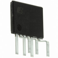
7-SIP, 6 Leads, Exposed Pad, Formed Leads
Operating Temperature
-40°C ~ 150°C
Current - Output / Channel
*
Internal Switch(s)
Yes
Efficiency
85%
Operating Supply Voltage
36 V
Maximum Supply Current
2.25 mA
Maximum Power Dissipation
12 W
Maximum Operating Temperature
+ 125 C
Mounting Style
Through Hole
Minimum Operating Temperature
- 20 C
Lead Free Status / RoHS Status
Lead free / RoHS Compliant
Other names
596-1300-5
Available stocks
Company
Part Number
Manufacturer
Quantity
Price

Part Number:
LNK403EG
Manufacturer:
POWER
Quantity:
20 000


Pin Functional Description
DRAIN (D) Pin:
This pin is the power MOSFET drain connection. It also
provides internal operating current for both start-up and
steady-state operation.
SOURCE (S) Pin:
This pin is the power MOSFET source connection. It is also the
ground reference for the BYPASS, FEEDBACK, REFERENCE and
VOLTAGE MONITOR pins.
BYPASS (BP) Pin:
This is the connection point for an external bypass capacitor for
the internally generated 5.9 V supply. This pin also provides
output power selection through choice of the BYPASS pin
capacitor value.
FEEDBACK (FB) Pin:
The FEEDBACK pin is used for output voltage feedback. The
current into the FEEDBACK pin is directly proportional to the
output voltage. The FEEDBACK pin also includes circuitry to
protect against open load and overload output conditions.
REFERENCE (R) Pin:
This pin is connected to an external precision resistor and is
used to configure for dimming (LNK403-409) and non-TRIAC
dimming (LNK413-419) modes of operation.
Rev. C 11/10
Figure 2.
LNK403-409EG/413-419EG
FEEDBACK (FB)
REFERENCE (R)
2
BYPASS (BP)
MONITOR (V)
VOLTAGE
Functional Block Diagram.
6.4 V
FEEDBACK
SENSE
SENSE
LINE
3-V
V
BG
1 V
T
UV/OV
I
CAPACITOR
LIM
BYPASS
SELECT
LOGIC
STOP
DC
FB
OFF
MAX
M
I
I
I
V
OSCILLATOR
FB
CLOCK
JITTER
REFERENCE
AUTO-RESTART
CONTROL
SOFT-START
PFC/CC
BLOCK
COUNTER
TIMER
+
-
Comparator
M
PRESENT
V
BG
I
VOLTAGE MONITOR (V) Pin:
This pin interfaces with an external input line peak detector,
consisting of a rectifier, filter capacitor and resistors. The
applied current is used to control stop logic for line under-
voltage (UV), overvoltage (OV), provide feed-forward to control
the output current and the remote ON/OFF function.
FAULT
Figure 3.
DC
FB
MAX
OFF
Exposed Pad
(backside) Internally
Connected to
SOURCE Pin (see
eSIP-7C Package
Drawing)
5.9 V
5.0 V
Pin Configuration.
UNDERVOLTAGE
BYPASS PIN
+
-
OCP
REGULATOR
HYSTERETIC
SHUTDOWN
THERMAL
E Package (eSIP-7C)
5.9 V
CURRENT LIMIT
COMPARATOR
(Top View)
Driver
Gate
PI-5431-102610
SenseFet
+
-
V
LEB
SENSE
www.powerint.com
I
LIM
I
S
7 D
5 S
4 BP
3 FB
2 V
1 R
PI-5432-060710
SOURCE (S)
DRAIN (D)
Related parts for LNK403EG
Image
Part Number
Description
Manufacturer
Datasheet
Request
R

Part Number:
Description:
Led Driver Ic With Triac Dimming, Single-stage Pfc And Primary-side Constant Current Control
Manufacturer:
Power Integrations, Inc.
Datasheet:

Part Number:
Description:
SOP-16
Manufacturer:
Power Integrations
Datasheet:
Part Number:
Description:
DIP8
Manufacturer:
Power Integrations
Datasheet:
Part Number:
Description:
TO-263
Manufacturer:
Power Integrations
Datasheet:
Part Number:
Description:
TO-263
Manufacturer:
Power Integrations
Datasheet: