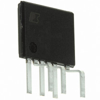
LNK403EG Power Integrations, LNK403EG Datasheet - Page 5

LNK403EG
Manufacturer Part Number
LNK403EG
Description
IC LED DVR TRIAC 12W DIM SIP-7C
Manufacturer
Power Integrations
Series
LinkSwitch®-PHr
Datasheet
1.LNK403EG.pdf
(20 pages)
Specifications of LNK403EG
Constant Current
Yes
Topology
PWM
Number Of Outputs
1
Internal Driver
Yes
Type - Primary
*
Type - Secondary
*
Frequency
62kHz ~ 70kHz
Voltage - Supply
90 V ~ 265 V
Voltage - Output
*
Mounting Type
Through Hole
Package / Case
7-SIP, 6 Leads, Exposed Pad, Formed Leads
Operating Temperature
-40°C ~ 150°C
Current - Output / Channel
*
Internal Switch(s)
Yes
Efficiency
85%
Operating Supply Voltage
36 V
Maximum Supply Current
2.25 mA
Maximum Power Dissipation
12 W
Maximum Operating Temperature
+ 125 C
Mounting Style
Through Hole
Minimum Operating Temperature
- 20 C
Lead Free Status / RoHS Status
Lead free / RoHS Compliant
Other names
596-1300-5
Available stocks
Company
Part Number
Manufacturer
Quantity
Price
Part Number:
LNK403EG
Manufacturer:
POWER
Quantity:
20 000
Application Example
14 W TRIAC Dimmable High Power Factor LED Driver
Design Example
The circuit schematic in Figure 6 shows a TRIAC dimmable high
power-factor LED driver based on LNK406EG from the
LinkSwitch-PH family of devices. It was optimized to drive an
LED string at a voltage of 28 V with a constant current of 0.5 A
(±5%) ideal for PAR lamp retro-fit applications. The design
operates over a universal input voltage range of 90 VAC to
265 VAC but provides the specified output current tolerance
over a line voltage range of 90 VAC to 132 VAC (this is configurable
for high line only applications by simple component value changes).
The key goals of this design were compatibility with standard
leading edge TRIAC AC dimmers, very wide dimming range
(1000:1, 500 mA:0.5 mA), high efficiency (>85%) and high power
factor (>0.9). The design is fully protected from faults such as
no-load, overload and output short-circuit conditions and over
temperature.
Circuit Description
The LinkSwitch-PH device (U1) integrates the power MOSFET,
controller and start-up functions into a single package reducing
the component count versus typical implementations. Configured
as part of an isolated continuous conduction mode flyback
converter, U1 provides high power factor via its internal control
algorithm together with the small input capacitance of the
design. Continuous conduction mode operation results in
reduced primary peak and RMS current. This both reduces
EMI noise, allowing simpler, smaller EMI filtering components and
improves efficiency. Output current regulation is maintained
without the need for secondary side sensing which eliminates
current sense resistors and improves efficiency.
Figure 6.
www.powerint.com
90 - 265
VAC
N
L
3.15 A
275 VAC
F1
RV1
Schematic of an Isolated, TRIAC Dimmable, High Power Factor, Universal Input, 14 W LED Driver.
1000 µH
1000 µH
1 kΩ
1 kΩ
R16
R17
L1
L2
275 VAC
47 nF
C1
2KBP06M
600 V
1000 µH
BR1
2.4 MΩ
L3
R11
750 kΩ
750 kΩ
R10
R9
1%
1%
FMMT558
DL4002
D1
Q1
15 nF
50 V
C6
15 Ω
R12
1%
ZMM5245B-7
VR2
15 V
130 Ω
1/2 W
R13
IRFR310
Q2
220 nF
510 Ω
630 V
R18
1 W
C11
100 nF
630 V
240 kΩ
C2
1/2 W
R1
LinkSwitch-PH
400 V
1 µF
C3
Input Stage
Fuse F1 provides protection from component failures while RV1
provides a clamp during differential line surges, keeping the
peak drain voltage of U1 below the 725 V rating of the internal
power MOSFET. Bridge rectifier BR1 rectifies the AC line
voltage. EMI filtering is provided by L1-L3, C1, R16 and R17
together with the safety rated Y class capacitor (C7) that bridges
the safety isolation barrier between primary and secondary.
Resistor R16 and R17 act to damp any resonances formed
between L1, L2, C1 and the AC line impedance. A small bulk
capacitor (C2) is required to provide a low impedance source for
the primary switching current. The maximum value of C1 and
C2 is limited in order to maintain a power factor of greater than 0.9.
LinkSwitch-PH Primary
To provide peak line voltage information to U1 the incoming
rectified AC peak charges C3 via D2. This is then fed into the
VOLTAGE MONITOR pin of U1 as a current via R2 and R3. This
sensed current is also used by the device to set the line input
overvoltage and undervoltage protection thresholds. Resistor
R1 provides a discharge path for C3 with a time constant much
longer than that of the rectified AC to prevent generation of line
frequency ripple.
The VOLTAGE MONITOR pin current and the FEEDBACK pin
current are used internally to control the average output LED
current. For TRIAC phase-dimming applications a 49.9 kW
resistor (R4) is used on the REFERENCE pin and 4 MW (R2+R3)
on the VOLTAGE MONITOR pin to provide a linear relationship
between input voltage and the output current and maximizing
the dimming range. Resistor R4 also sets the internal line input
undervoltage and overvoltage protection thresholds.
DL4007
LNK406EG
D2
2 MΩ
2 MΩ
1%
1%
R2
R3
U1
D
S
UF4002
P6KE200A
UF4007
CONTROL
D4
D3
VR1
R
49.9 kΩ
V
R4
1%
1N4148
FB
D5
BP
3 kΩ
10 µF
16 V
R5
C4
162 kΩ
MMBT3904
1%
1 kΩ
R6
R19
Q3
LNK403-409EG/413-419EG
11
100 nF
1
50 V
C13
RM8
T1
ZMM5259B-7
FL1
FL2
3
2
10 kΩ
R20
VR3
39 V
MBRS4201T3G
D8
1 µF
50 V
BAV21WS-7-F
C12
150 Ω
R8
D7
330 µF
DL4936
50 V
C8
D6
330 µF
50 V
C10
10 kΩ
R7
20 kΩ
R15
250 VAC
22 µF
50 V
2.2 nF
C5
C7
28 V, 500 mA
Rev. B 11/10
PI-5997-061510
RTN
5


