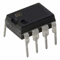
L6569 STMicroelectronics, L6569 Datasheet

L6569
Specifications of L6569
Available stocks
Related parts for L6569
L6569 Summary of contents
Page 1
... The output drivers are designed to drive external n- channel power MOSFET and IGBT. The internal log- ic assures a dead time [typ. 1. avoid cross- conduction of the power devices. Two version are available: L6569 and L6569A. They differ in the low voltage gate driver start up sequence ...
Page 2
... L6569 L6569A ABSOLUTE MAXIMUM RATINGS Symbol I (*) Supply Current S V Oscillator Resistor Voltage CF V Low Side Switch Gate Output LVG V High Side Switch Source Output OUT V High Side Switch Gate Output HVG V Floating Supply Voltage BOOT V Floating Supply vs OUT Voltage BOOT/OUT dV /dt ...
Page 3
... RF Oscillator timing resistor pin. A buffer set alternatively to V connected between pin 2 and 3. Alternatively, the signal on pin 2 can be used also to drive another IC (i.e. another L6569 to drive a full H-bridge Oscillator timing capacitor pin. A capacitor connected between this pin and GND fixes (together with R frequency Alternatively an external logic signal can be applied to the pin to drive the IC ...
Page 4
... L6569 L6569A ELECTRICAL CHARACTERISTCS (continued) Symbol Pin Parameter High Level Output Voltage RFO V RF Low Level Output Voltage RF OFF Upper Threshold CFU V CF Lower Threshold CFL t Internal Dead Time d DC Duty Cycle, Ratio Between Dead Time + Conduction Time of High Side and Low Side Drivers ...
Page 5
... Bootstrap Function The L6569 has an internal Bootstrap structure that enables the user to avoid the external diode needed, in sim- ilar devices, to perform the charge of the bootstrap capacitor that, in turns, provide an appropriate driving to the Upper External Mosfet. The operation is achieved with an unique structure (patented) that uses a High Voltage Lateral DMOS driven by an internal charge pump (see Block Diagram) and synchronized, with a 50 nsec delay, with the Low Side Gate driver (LVG pin), actually working as a synchronous rectifier ...
Page 6
... L6569 L6569A DEMO BOARD To allow an easy evaluation of the device, a P.C. board dedicated to lamp ballast application has been de- signed. Fig.11 shows the electrical schematic of a typical ballast application, while the PC and component layout is giv Fig12. This application has been designed to work with both the 110+/-20%V and the 220 +/- 20%V mains by means of a voltage doubler configuration at the bulk capacitor ...
Page 7
... Figure 2. Waveforms (L6569 BOOT OUT V CF LVG Figure 3. Waveforms (L6569A BOOT OUT V CF LVG =Ron*C BOOT =Ron*C BOOT L6569 L6569A V SUVP V S 4.6V(typ) D95IN250B V SUVP V S 4.6V(typ) D95IN251B 7/13 ...
Page 8
... L6569 L6569A Figure 4. Typical Dead Time vs. Temperature Dependency Dead time [ sec] 1.7 1.6 1.5 1.4 1.3 1.2 1.1 1 0.9 - Temperature [C] Figure 5. Typical Frequency vs Temperature Dependency Frequency [KHz -50 - Temperature [C] Figure 6. Typical and Theoretical Oscillator Frequency vs Resistor Value f (KHz) 150 100 90 C=330pF 80 C=560pF ...
Page 9
... BOOT S RF HVG 1/4W L6569 OUT 27K 1/ 1/4W LVG C1 GND 560pF D8 50V C9 470pF 630V 1N4148 R6 47 1/4W D1 ZPD 18V D96IN419B L6569 L6569A Q1 R9 STD2NB50-1 180K 1/4W R10 10K 1/4W L1=2.4mH Q2 C7 STD2NB50-1 8.2nF 630V 180K 100nF 8.2nF 1/4W 250V 630V BYW100-100 ...
Page 10
... L6569 L6569A Figure 12. PC Board and Components Layout. 10/13 Component Side Copper Side ...
Page 11
... D and F do not include mold flash or protrusions. Mold flash or potrusions shall not exceed 0.15mm (.006inch). inch TYP. MAX. MECHANICAL DATA 0.069 0.010 0.065 0.033 0.019 0.010 0.020 0.197 0.244 0.050 0.150 0.157 0.050 0.024 L6569 L6569A OUTLINE AND SO8 11/13 ...
Page 12
... L6569 L6569A mm DIM. MIN. TYP. MAX. A 3.32 a1 0.51 B 1.15 1.65 b 0.356 0.55 b1 0.204 0.304 D 10.92 E 7.95 9.75 e 2.54 e3 7.62 e4 7.62 F 6.6 I 5.08 L 3.18 3.81 Z 1.52 12/13 inch MIN. TYP. MAX. 0.131 0.020 0.045 0.065 0.014 0.022 0.008 0.012 0.430 0.313 0.384 ...
Page 13
... STMicroelectronics. The ST logo is a registered trademark of STMicroelectronics Australia - Brazil - China - Finland - France - Germany - Hong Kong - India - Italy - Japan - Malaysia - Malta - Morocco - Singapore - Spain 2000 STMicroelectronics - All Rights Reserved STMicroelectronics GROUP OF COMPANIES - Sweden - Switzerland - United Kingdom - U.S.A. http://www.st.com L6569 L6569A 13/13 ...


