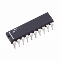
LT1161CN Linear Technology, LT1161CN Datasheet - Page 5

LT1161CN
Manufacturer Part Number
LT1161CN
Description
IC MOSFET DRIVER N-CH QUAD 20DIP
Manufacturer
Linear Technology
Datasheet
1.LT1161CSWPBF.pdf
(12 pages)
Specifications of LT1161CN
Configuration
High-Side
Input Type
Non-Inverting
Delay Time
220µs
Number Of Configurations
4
Number Of Outputs
4
Voltage - Supply
8 V ~ 48 V
Operating Temperature
0°C ~ 70°C
Mounting Type
Through Hole
Package / Case
20-DIP (0.300", 7.62mm)
Lead Free Status / RoHS Status
Contains lead / RoHS non-compliant
Current - Peak
-
High Side Voltage - Max (bootstrap)
-
Available stocks
Company
Part Number
Manufacturer
Quantity
Price
Part Number:
LT1161CN
Manufacturer:
LT/凌特
Quantity:
20 000
Part Number:
LT1161CN#PBF
Manufacturer:
LINEAR/凌特
Quantity:
20 000
OPERATIO
Input/Supply Sequencing
There are no input/supply sequencing requirements for
the LT1161. The input may be taken up to 15V with the
supply at 0V. When the supply is turned on with an input
high, the MOSFET turn-on will be inhibited until the timing
capacitor charges to 3V (i.e., for one restart cycle). The
two V
other.
Isolating the Inputs
Operation in harsh environments may require isolation to
prevent ground transients from damaging control logic.
The LT1161 easily interfaces to low cost opto-isolators.
The network shown in Figure 3 ensures that the input will
be pulled above 2V, but not exceed the absolute maximum
The LT1161 gate pin has two states, OFF and ON. In the
OFF state it is held low, while in the ON state it is pumped
to 12V above supply by a self-contained 750kHz charge
pump. The OFF state is activated when either the input pin
is below 1.4V or the timer pin is below 3V. Conversely, for
the ON state to be activated, both the input and timer pins
must be above their thresholds.
If left open, the input pin is held low by a 75k resistor, while
the timer pin is held a diode drop above 3V by a 14µA pull-
up current source. Thus the timer pin automatically re-
verts to the ON state, subject to the input also being high.
The input has approximately 200mV of hysteresis.
The sense pin normally connects to the drain of the power
MOSFET, which returns through a low valued drain sense
resistor to supply. When the gate is ON and the MOSFET
drain current exceeds the level required to generate a
65mV drop across the drain sense resistor, the sense
comparator activates a pull-down NPN which rapidly pulls
the timer pin below 3V. This in turn causes the timer
comparator to override the input pin and activate the gate
pin OFF state, thus protecting the power MOSFET. In order
for the sense comparator to accurately sense MOSFET
drain current, the LT1161 supply pins must be connected
directly to the positive side of the drain sense resistors.
APPLICATIONS
+
pins (11, 20) must always be connected to each
U
U
(Each Channel, Refer to Functional Diagram)
INFORMATION
U
W
U
When the MOSFET gate voltage is less than 1.4V, the timer
pin is released. The 14µA current source then slowly
charges the timing capacitor back to 3V where the charge
pump again starts to drive the gate pin high. If a fault still
exists, such as a short circuit, the sense comparator
threshold will again be exceeded and the timer cycle will
repeat until the fault is removed (see Figure 2).
rating, for supply voltages of 12V to 48V over the entire
temperature range. In order to maintain the OFF state, the
opto must have less than 20µA of dark current (leakage)
hot.
TIMER
INPUT
GATE
LOGIC
INPUT
0V
0V
V
3V
+
OFF
12V
2k
LOGIC
GND
Figure 3. Isolating the Inputs
NORMAL
Figure 2. Timing Diagram
1/4 NEC PS2501-4
GROUND
POWER
OVERCURRENT
12V TO 48V
100k
51k
IN
GND
GND
LT1161
LT1161
1161 F03
NORMAL
1161fa
1161 F02
5


