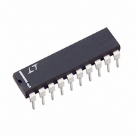
LT1161CN Linear Technology, LT1161CN Datasheet - Page 6

LT1161CN
Manufacturer Part Number
LT1161CN
Description
IC MOSFET DRIVER N-CH QUAD 20DIP
Manufacturer
Linear Technology
Datasheet
1.LT1161CSWPBF.pdf
(12 pages)
Specifications of LT1161CN
Configuration
High-Side
Input Type
Non-Inverting
Delay Time
220µs
Number Of Configurations
4
Number Of Outputs
4
Voltage - Supply
8 V ~ 48 V
Operating Temperature
0°C ~ 70°C
Mounting Type
Through Hole
Package / Case
20-DIP (0.300", 7.62mm)
Lead Free Status / RoHS Status
Contains lead / RoHS non-compliant
Current - Peak
-
High Side Voltage - Max (bootstrap)
-
Available stocks
Company
Part Number
Manufacturer
Quantity
Price
Part Number:
LT1161CN
Manufacturer:
LT/凌特
Quantity:
20 000
Part Number:
LT1161CN#PBF
Manufacturer:
LINEAR/凌特
Quantity:
20 000
APPLICATIONS
Drain Sense Configuration
The LT1161 uses supply-referenced current sensing. One
input of each channel’s current-sense comparator is con-
nected to a drain sense pin, while the second input is offset
65mV below the supply bus inside the device. For this
reason, Pins 11 and 20 of the LT1161 must be treated not
only as supply pins, but as the reference inputs for the
current-sense comparators.
Figure 4 shows the proper drain sense configuration for
the LT1161. Note that the sense pin goes to the drain end
of the sense resistor, while the two V
other and connected to supply at the same point as the
positive ends of the sense resistors. Local supply
decoupling at the LT1161 is important at high input
voltages (see Protecting Against Supply Transients).
The drain sense threshold voltage has a positive tempera-
ture coefficient, allowing PTC sense resistors to be used
(see Printed Circuit Board Shunts). The selection of R
should be based on the minimum threshold voltage:
Thus the 0.02Ω drain sense resistor in Figure 4 would yield
a minimum trip current of 2.5A. This simple configuration
is appropriate for resistive or inductive loads which do not
generate large current transients at turn-on.
LT1161
6
1µF
C
T
R
S
=
50
I
T1
SET
mV
LT1161
Figure 4. Drain Sense Configuration
GND
GND
DS1
V
V
G1
U
+
+
+
INFORMATION
U
10µF
0.02Ω
(PTC)
W
R
+
S
pins are tied to each
24V
IRFZ34
24V, 2A
SOLENOID
U
+
100µF
50V
1161 F04
S
Automatic Restart Period
The timing capacitor C
length of time the power MOSFET is held off following a
current limit trip. Curves are given in the Typical Perfor-
mance Characteristics to show the restart period for
various values of C
50ms restart period.
Defeating Automatic Restart
Some applications are required to remain off after a fault
occurs. When the LT1161 is being driven from CMOS
logic, this can be easily implemented by connecting
resistor R1 between the input and timer pins as shown in
Figure 5. R1 supplies the sustaining current for an SCR
which latches the timer pin low. This prevents the MOSFET
gate from turning ON until the input has been recycled.
Inductive vs Capacitive Loads
Turning on an inductive load produces a relatively benign
ramp in MOSFET current. However, when an inductive
load is turned off, the current stored in the inductor needs
somewhere to decay. A clamp diode connected directly
across each inductive load normally serves this purpose.
If a diode is not employed the LT1161 clamps the MOSFET
gate 0.7V below ground. This causes the MOSFET to
resume conduction during the current decay with (V
V
Capacitive loads exhibit the opposite behavior. Any load
that includes a decoupling capacitor will generate a cur-
rent equal to C
With large electrolytic capacitors, the resulting current
GS
Figure 5. Latch-Off Input Network (Auto-Restart Defeated)
+ 0.7V) across it, resulting in high dissipation peaks.
LOGIC
CMOS
5V
LOAD
OFF = 0V
T
ON = 5V
. For example, C
× (∂V/∂t) during capacitor in-rush.
T
shown in Figure 4 determines the
R1
2k
TIMER
INPUT
LT1161
T
= 0.33µF yields a
1161 F05
1161fa
+
+


