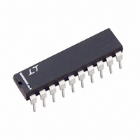
LT1161CN Linear Technology, LT1161CN Datasheet - Page 7

LT1161CN
Manufacturer Part Number
LT1161CN
Description
IC MOSFET DRIVER N-CH QUAD 20DIP
Manufacturer
Linear Technology
Datasheet
1.LT1161CSWPBF.pdf
(12 pages)
Specifications of LT1161CN
Configuration
High-Side
Input Type
Non-Inverting
Delay Time
220µs
Number Of Configurations
4
Number Of Outputs
4
Voltage - Supply
8 V ~ 48 V
Operating Temperature
0°C ~ 70°C
Mounting Type
Through Hole
Package / Case
20-DIP (0.300", 7.62mm)
Lead Free Status / RoHS Status
Contains lead / RoHS non-compliant
Current - Peak
-
High Side Voltage - Max (bootstrap)
-
Available stocks
Company
Part Number
Manufacturer
Quantity
Price
Part Number:
LT1161CN
Manufacturer:
LT/凌特
Quantity:
20 000
Part Number:
LT1161CN#PBF
Manufacturer:
LINEAR/凌特
Quantity:
20 000
APPLICATIONS
spike can play havoc with the power supply and false trip
the current-sense comparator.
Turn-on ∂V/∂t is controlled by the addition of the simple
network shown in Figure 6. This network takes advantage
of the fact that the MOSFET acts as a source follower
during turn-on. Thus the ∂V/∂t on the source can be
controlled by controlling the ∂V/∂t on the gate:
where V
ing C
spike. For example, if V
∂V/∂t = 2.2V/ms, resulting in a 2.2A turn-on spike into
1000µF. The diode and second resistor in the network
ensure fast current limit turn-off.
When turning off a capacitive load, the source of the
MOSFET can “hang up” if the load resistance does not
discharge C
If this is the case, a diode may have to be added from
source to gate to prevent V
Adding Current Limit Delay
When capacitive loads are being switched or in very noisy
environments, it is desirable to add delay in the drain
current-sense path to prevent false tripping (inductive
loads normally do not need delay). This is accomplished
by the current limit delay network shown in Figure 6. R
∂
∂
V
t
LOAD
=
LT1161
TH
Figure 6. ∂V/∂t Control and Current Limit Delay
V
10
times this ∂V/∂t yields the value of the current
is the MOSFET gate threshold voltage. Multiply-
+
LOAD
5
−
DS
V
V
×
G
+
+
V
C
TH
as fast as the gate is being pulled down.
1
U
∂V/∂t CONTROL NETWORK
+
DELAY NETWORK
100k
= 24V, V
CURRENT LIMIT
C
INFORMATION
D
U
GS(MAX)
R
D
1N4148
(≤10k)
100k
C1
TH
1N4148
W
from being exceeded.
= 2V, and C1 = 0.1µF,
+
24V
U
1RFZ24
C
1161 F06
LOAD
+
D
and C
approximately 10 × I
and provides immediate turn-off (see Figure 7). To ensure
proper operation of the timer, C
Printed Circuit Board Shunts
The sheet resistance of 1oz. copper clad is approximately
5 × 10
+0.39%/°C. Since the LT1161 drain sense threshold has a
similar temperature coefficient (+0.33%/°C), this offers
the possibility of nearly zero TC current sensing using
“free” drain sense resistors made out of PC trace material.
A conservative approach is to use 0.02" of width for each
1A of current for 1oz. copper. Combining the LT1161 drain
sense threshold with the 1oz. copper sheet resistance
results in a simple expression for width and length:
The width for 2oz. copper would be halved while the length
would remain the same.
Bends may be incorporated into the resistor to reduce
space; each bend is equivalent to approximately 0.6 ×
width of straight length. Kelvin connections should be
employed by running separate traces from the ends of the
resistors back to the LT1161 V
Application Note 53 for further information on printed
circuit board shunts.
Width (1oz. Cu) = 0.02" × I
Length (1oz. Cu) = 2"
D
delay the overcurrent trip for drain currents up to
–4
0.01
Ω/square with a temperature coefficient of
0.1
10
1
1
Figure 7. Current Limit Delay Time
MOSFET DRAIN CURRENT (1 = SET CURRENT)
SET
, above which the diode conducts
10
SET
D
+
must be ≤ C
and sense pins. See
L1161 F07
100
LT1161
T
.
1161fa
7


