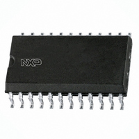
UBA2032T/N2,118 NXP Semiconductors, UBA2032T/N2,118 Datasheet - Page 5

UBA2032T/N2,118
Manufacturer Part Number
UBA2032T/N2,118
Description
IC DRIVER FULL BRIDGE SO-24
Manufacturer
NXP Semiconductors
Datasheet
1.UBA2032TSN3118.pdf
(21 pages)
Specifications of UBA2032T/N2,118
Configuration
H Bridge
Input Type
Self Oscillating
Current - Peak
130mA
Number Of Configurations
1
Number Of Outputs
4
High Side Voltage - Max (bootstrap)
550V
Voltage - Supply
10.5 V ~ 13.5 V
Operating Temperature
-40°C ~ 150°C
Mounting Type
Surface Mount
Package / Case
24-SOIC (7.5mm Width)
Lead Free Status / RoHS Status
Lead free / RoHS Compliant
Delay Time
-
Other names
935270516118
UBA2032TD-T
UBA2032TD-T
UBA2032TD-T
UBA2032TD-T
Philips Semiconductors
FUNCTIONAL DESCRIPTION
Supply voltage
The UBA2032 is powered by a supply voltage applied to
pin HV, for instance the supply voltage of the full bridge.
The IC generates its own low supply voltage for the
internal circuitry. Therefore an additional low voltage
supply is not required. A capacitor has to be connected to
pin V
circuit can also be powered by a low voltage supply directly
applied to pin V
connected to pin V
Start-up
With an increasing supply voltage the IC enters the
start-up state; the higher power transistors are kept off and
the lower power transistors are switched on. During the
start-up state the bootstrap capacitors are charged and the
bridge output current is zero. The start-up state is defined
until V
Voltage Lock-Out. The state of the outputs during the
start-up phase is overruled by the bridge disable function.
2005 Mar 24
handbook, halfpage
Full bridge driver IC
DD
DD
to obtain a ripple-free internal supply voltage. The
= V
DD(UVLO)
Fig.2 Pin configuration (SO24).
EXTDR
SGND
V DD
DD
LVS
LVS
n.c.
n.c.
DD
RC
HV
SU
BD
. In this case pin HV should be
DD
10
11
12
1
2
3
4
5
6
7
8
9
, where UVLO stands for Under
or pin SGND.
UBA2032T
MGU543
24
23
22
21
20
19
18
17
16
15
14
13
GHR
FSR
SHR
n.c.
GLR
n.c.
PGND
GLL
n.c.
SHL
FSL
GHL
5
Release of the power drive
At the moment the supply voltage on pin V
exceeds the level of release power drive, the output
voltage of the bridge depends on the control signal on
pin EXTDR; see Table 1. The bridge position after
start-up, disable or delayed start-up (via pin SU), depends
on the status of pin DD and pin EXTDR. If pin DD = LOW
(divider enabled) the bridge will start in the pre-defined
position pin GLR and pin GHL = HIGH and pin GLL and
pin GHR = LOW. If pin DD = HIGH (divider disabled) the
bridge position will depend on the status of pin EXTDR.
If the supply voltage on pin V
drops below the reset level of power drive the IC enters the
start-up state again.
Oscillation
At the point where the supply voltage on pin HV crosses
the level of release power drive, the bridge begins
commutating between the following two defined states:
handbook, halfpage
Higher left and lower right MOSFETs on,
higher right and lower left MOSFETs off
Higher left and lower right MOSFETs off,
higher right and lower left MOSFETs on.
Fig.3 Pin configuration (SSOP28).
EXTDR
SGND
V DD
LVS
LVS
n.c.
n.c.
n.c.
n.c.
DD
RC
HV
SU
BD
10
11
12
13
14
1
2
3
4
5
6
7
8
9
UBA2032TS
DD
MGU544
or pin HV decreases and
28
27
26
25
24
23
22
21
20
19
18
17
16
15
Product specification
GHR
FSR
SHR
n.c.
n.c.
GLR
n.c.
PGND
GLL
n.c.
n.c.
SHL
FSL
GHL
UBA2032
DD
or pin HV


