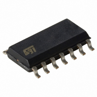
L6393D STMicroelectronics, L6393D Datasheet - Page 5

L6393D
Manufacturer Part Number
L6393D
Description
IC GATE DRIVER HALF BRDGE SOIC14
Manufacturer
STMicroelectronics
Type
High Side/Low Sider
Datasheet
1.L6393DTR.pdf
(19 pages)
Specifications of L6393D
Configuration
Half Bridge
Input Type
Non-Inverting
Delay Time
125ns
Current - Peak
270mA
Number Of Configurations
1
Number Of Outputs
2
High Side Voltage - Max (bootstrap)
600V
Operating Temperature
-40°C ~ 125°C
Mounting Type
Surface Mount
Package / Case
14-SOIC (3.9mm Width), 14-SOL
Product
Half-Bridge Drivers
Rise Time
75 ns
Fall Time
35 ns
Propagation Delay Time
125 ns
Supply Voltage (max)
21 V
Supply Voltage (min)
- 0.3 V
Supply Current
270 mA
Maximum Power Dissipation
800 mW
Maximum Operating Temperature
+ 125 C
Mounting Style
SMD/SMT
Bridge Type
Half Bridge
Maximum Turn-off Delay Time
200 ns
Maximum Turn-on Delay Time
200 ns
Minimum Operating Temperature
- 40 C
Number Of Drivers
1
Output Voltage
580 V
Lead Free Status / RoHS Status
Lead free / RoHS Compliant
Voltage - Supply
-
Lead Free Status / Rohs Status
Lead free / RoHS Compliant
Available stocks
Company
Part Number
Manufacturer
Quantity
Price
Part Number:
L6393D
Manufacturer:
ST
Quantity:
20 000
L6393
3
Note:
Note:
Truth table
Table 3.
X: don’t care
In the L6393 IC the two input signals PHASE and BRAKE are fed into an AND logic port and
the resulting signal is in phase with the high side output HVG and in opposition of phase with
the low side output LVG. This means that if BRAKE is kept to high level, the PHASE signal
drives the half-bridge in phase with the HVG output and in opposition of phase with the LVG
output. If BRAKE is set to low level the low side output LVG is always ON and the high side
output HVG is always OFF, whatever the PHASE signal. This kind of logic interface provides
the possibility to control the power stages using the PHASE signal to select the current
direction in the bridge and the BRAKE signal to perform current slow decay on the low sides.
From the point of view of the logic operations the two signals PHASE and BRAKE are
completely equivalent, that means the two signals can be exchanged without any change in
the behavior on the resulting output signals (see the
The dead time between the turn OFF of one power switch and the turn ON of the other
power switch is defined by the resistor connected between DT pin and the ground.
SD
H
H
H
H
L
Truth table
PHASE
Inputs
H
H
X
L
L
Doc ID 14497 Rev 4
BRAKE
X
H
H
L
L
Figure 1 on page
LVG
H
H
H
L
L
Outputs
3).
Truth table
HVG
H
L
L
L
L
5/19


