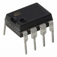
TDE1798DP STMicroelectronics, TDE1798DP Datasheet

TDE1798DP
Specifications of TDE1798DP
Available stocks
Related parts for TDE1798DP
TDE1798DP Summary of contents
Page 1
... If internal dissipation becomes too high, PIN CONNECTION (Top view) September 2003 0.5A INTELLIGENT POWER SWITCH ORDERING NUMBER: TDE1798DP CC the driver will shut down to prevent excessive heating. The output stays null after the overload is off, if the reset input is low. If high, the output will alternatively switch on and off until the overload is removed ...
Page 2
TDE1798 ABSOLUTE MAXIMUM RATINGS Symbol V Supply Voltage CC V Input Differential Voltage ID V Input Voltage I V Reset Input Voltage I(reset) I Output Current O P Power Dissipation tot Reset Input Sink Current (in thermal shut-down) W Repetitive ...
Page 3
THERMAL DATA Symbol R Thermal Resistance Junction-case (1) th j-case R Thermal Resistance Junction-ambient (1) th j-ambient 2 1) Devices bounded on a 40cm glass-epoxy printed circuit 0.15cm thick with 4cm ELECTRICAL CHARACTERISTICS (note 2) TDE - +85 ...
Page 4
TDE1798 4/14 ...
Page 5
TYPICAL APPLICATION AUTOMATIC RESET (*) D1 and Z1 needed if the demagnetization energy is higher than 150mJ SHORT CIRCUIT CONDITIONS WITH AUTOMATIC RESET TYPICAL APPLICATION CONTROLLED RESET TDE1798 5/14 ...
Page 6
TDE1798 SHORT CIRCUIT CONDITIONS WITH CONTROLLED RESET DEMAGNETIZATION OF INDUCTIVE LOADS WITHOUT EXTERNAL CLAMPING DEVICES. With no external clamping device, the energy of demagnetization is dissipated in the TDE1798 output stage, and the clamping voltage is the col ...
Page 7
A 1 AMP. DRIVER (reset may be either automatic or controlled) ALARM OUTPUT SINK ALARM OUTPUT SOURCE TDE1798 7/14 ...
Page 8
TDE1798 PARALLEL ALARM OUTPUTS INTERFACE BETWEEN HIGH VOLTAGE AND LOW VOLTAGE SYSTEM 8/14 ...
Page 9
RESET AND SYNCHRONIZATION Recommended diagram when the outputs are in parallel. After thermal disjunction a restart is pos- SYNCRONOUS AUTOMATIC RESET (parallel or independent outputs) SYNCHRONOUS CONTROLLED RESET (parallel or idependent outputs) sible when all the circuits are returned in ...
Page 10
TDE1798 TWO QUADRANTS D.C. MOTOR DRIVE MAIN FEATURES 50V CC CC Maximum output current 0.5A Full protection against overloads and short-cir- cuits No need of deadtime during rotation reversing TTL compatible inputs TDE1799 and TDE1798 input signals ...
Page 11
ON/OFF CYCLES ROTATION REVERSING TDE1798 11/14 ...
Page 12
TDE1798 OVERLOAD CONDITIONS 12/14 ...
Page 13
DIM. MIN. TYP. MAX. MIN. A 3.32 a1 0.51 0.020 B 1.15 1.65 0.045 b 0.356 0.55 0.014 b1 0.204 0.304 0.008 D 10.92 E 7.95 9.75 0.313 e 2.54 e3 7.62 e4 7.62 F 6.6 I 5.08 L ...
Page 14
... STMicroelectronics. Specifications mentioned in this publication are subject to change without notice. This publication supersedes and replaces all information previously supplied. STMicroelectronics products are not authorized for use as critical components in life support devices or systems without express written approval of STMicroelectronics. The ST logo is a registered trademark of STMicroelectronics. ...


