L6207D013TR STMicroelectronics, L6207D013TR Datasheet - Page 6
L6207D013TR
Manufacturer Part Number
L6207D013TR
Description
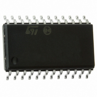
IC DRVR FULL BRDG DUAL 24-SOIC
Manufacturer
STMicroelectronics
Type
H Bridger
Series
-r
Datasheet
1.L6207D013TR.pdf
(23 pages)
Specifications of L6207D013TR
Input Type
Non-Inverting
Number Of Outputs
4
On-state Resistance
300 mOhm
Current - Output / Channel
2.8A
Current - Peak Output
5.6A
Voltage - Supply
8 V ~ 52 V
Operating Temperature
-25°C ~ 125°C
Mounting Type
Surface Mount
Package / Case
24-SOIC (7.5mm Width)
Operating Current
10mA
Operating Temperature Classification
Automotive
Package Type
SO
Operating Supply Voltage (min)
8V
Operating Supply Voltage (typ)
48V
Operating Supply Voltage (max)
52V
Operating Supply Voltage
8 V to 52 V
Supply Current
0.01 A
Mounting Style
SMD/SMT
For Use With
497-4934 - BOARD MOTOR STEPPER/DC L6207 DIP
Lead Free Status / RoHS Status
Lead free / RoHS Compliant
Other names
497-3644-2
Available stocks
Company
Part Number
Manufacturer
Quantity
Price

Part Number:
L6207D013TR
Manufacturer:
ST
Quantity:
20 000


L6207
ELECTRICAL CHARACTERISTICS (continued)
(T
(7)
(8)
(9)
(10)
6/23
Switching Characteristics
PWM Comparator and Monostable
I
Over Current Protection
t
t
Symbol
RCA,
OCD(OFF)
t
t
t
OCD(ON)
t
t
I
amb
R
D(on)EN
D(off)EN
t
ON(MIN)
V
t
D(on)IN
D(off)IN
SOVER
BLANK
t
t
I
PROP
t
RISE
FALL
BIAS
OPDR
f
offset
OFF
t
CP
dt
I
Tested at 25°C in a restricted range and guaranteed by characterization.
See Fig. 1.
Measured applying a voltage of 1V to pin SENSE and a voltage drop from 2V to 0V to pin VREF.
See Fig. 2.
RCB
= 25 °C, V
Enable to out turn ON delay time
Input to out turn ON delay time
Output rise time
Enable to out turn OFF delay time
Input to out turn OFF delay time
Output Fall Time
Dead Time Protection
Charge pump frequency
Source Current at pins RC
RC
Offset Voltage on Sense
Comparator
Turn OFF Propagation Delay
Internal Blanking Time on
SENSE pins
Minimum On Time
PWM Recirculation Time
Input Bias Current at pins VREF
and VREF
Input Supply Overcurrent
Protection Threshold
Open Drain ON Resistance
OCD Turn-on Delay Time (10)
OCD Turn-off Delay Time (10)
B
s
= 48V, unless otherwise specified)
B
Parameter
(8)
(8)
A
and
(9)
(8)
(8)
A
I
I
(dead time included)
I
I
I
I
-25°C<T
V
V
R
R
T
I = 4mA
I = 4mA; C
I = 4mA; C
LOAD
LOAD
LOAD
LOAD
LOAD
LOAD
j
RCA
REFA,
OFF
OFF
= -25°C to 125°C
= V
= 20K
= 100K
=2.8A, Resistive Load
=2.8A, Resistive Load
=2.8A, Resistive Load
=2.8A, Resistive Load
=2.8A, Resistive Load
=2.8A, Resistive Load
V
j
REFB
Test Conditions
RCB
<125°C
EN
EN
= 2.5V
< 100pF
< 100pF
= 0.5V
C
C
OFF
OFF
(7)
= 1nF
= 1nF
Min
100
300
0.5
3.5
40
40
4
Typ
250
550
600
500
200
100
1.6
0.6
5.5
1.5
5.6
±5
40
13
61
1
1
Max
400
250
800
250
7.1
10
60
1
2
MHz
Unit
mA
mV
µA
ns
µs
ns
ns
ns
ns
µs
ns
µs
µs
µs
µs
ns
ns
A
Related parts for L6207D013TR
Image
Part Number
Description
Manufacturer
Datasheet
Request
R

Part Number:
Description:
IC DRVR FULL BRIDGE DUAL 24-SOIC
Manufacturer:
STMicroelectronics
Datasheet:

Part Number:
Description:
STMicroelectronics [RIPPLE-CARRY BINARY COUNTER/DIVIDERS]
Manufacturer:
STMicroelectronics
Datasheet:
Part Number:
Description:
STMicroelectronics [LIQUID-CRYSTAL DISPLAY DRIVERS]
Manufacturer:
STMicroelectronics
Datasheet:

Part Number:
Description:
BOARD EVAL FOR MEMS SENSORS
Manufacturer:
STMicroelectronics
Datasheet:
Part Number:
Description:
NPN TRANSISTOR POWER MODULE
Manufacturer:
STMicroelectronics
Datasheet:
Part Number:
Description:
TURBOSWITCH ULTRA-FAST HIGH VOLTAGE DIODE
Manufacturer:
STMicroelectronics
Datasheet:
Part Number:
Description:
Manufacturer:
STMicroelectronics
Datasheet:
Part Number:
Description:
DIODE / SCR MODULE
Manufacturer:
STMicroelectronics
Datasheet:
Part Number:
Description:
DIODE / SCR MODULE
Manufacturer:
STMicroelectronics
Datasheet:
Part Number:
Description:
Search -----> STE16N100
Manufacturer:
STMicroelectronics
Datasheet:
Part Number:
Description:
Search ---> STE53NA50
Manufacturer:
STMicroelectronics
Datasheet:
Part Number:
Description:
NPN Transistor Power Module
Manufacturer:
STMicroelectronics
Datasheet: