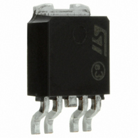
VN800PT-E STMicroelectronics, VN800PT-E Datasheet - Page 10

VN800PT-E
Manufacturer Part Number
VN800PT-E
Description
IC DRIVER HIGH SIDE 0.7A PPAK
Manufacturer
STMicroelectronics
Type
High Sider
Datasheet
1.VN800S-E.pdf
(24 pages)
Specifications of VN800PT-E
Input Type
Non-Inverting
Number Of Outputs
1
On-state Resistance
135 mOhm
Current - Output / Channel
700mA
Voltage - Supply
5.5 V ~ 36 V
Operating Temperature
-40°C ~ 150°C
Mounting Type
Surface Mount
Package / Case
PPAK (4 leads + tab)
Supply Voltage (min)
5.5 V
Supply Current
1.5 mA
Maximum Power Dissipation
41700 mW
Maximum Operating Temperature
+ 150 C
Mounting Style
SMD/SMT
Minimum Operating Temperature
- 40 C
Lead Free Status / RoHS Status
Lead free / RoHS Compliant
Current - Peak Output
-
Lead Free Status / Rohs Status
Lead free / RoHS Compliant
Available stocks
Company
Part Number
Manufacturer
Quantity
Price
VN800S-E / VN800PT-E
Figure 10. Application Schematic
GND
REVERSE BATTERY
Solution 1: Resistor in the ground line (R
can be used with any type of load.
The following is an indication on how to dimension the
R
where -I
be found in the absolute maximum rating section of the
device’s datasheet.
Power Dissipation in R
battery situations) is:
P
This resistor can be shared amongst several different
HSD. Please note that the value of this resistor should be
calculated with formula (1) where I
sum of the maximum on-state currents of the different
devices.
Please note that if the microprocessor ground is not
common with the device ground then the R
produce a shift (I
and the status output values. This shift will vary
depending on many devices are ON in the case of several
high side drivers sharing the same R
If the calculated power dissipation leads to a large
resistor or several devices have to share the same
resistor then the ST suggests to utilize Solution 2 (see
below).
Solution 2: A diode (D
A resistor (R
D
10/24
D
GND
GND
1) R
2) R
= (-V
24VDC
V
CC
resistor.
GND
GND
if the device will be driving an inductive load.
CC
GND
PROTECTION
)
2
/R
is the DC reverse ground pin current and can
600mV / (I
GND
GND
V
Volt.
Reg
CC
S(on)max
=1k
) / (-I
GND
5V
GND
S(on)max
GND
should be inserted in parallel to
* R
) in the ground line.
)
(when V
NETWORK
GND
).
BUS
ASIC
) in the input thresholds
S(on)max
CC
GND
<0: during reverse
.
GND
Rprot
Rprot
becomes the
STATUSn
AGAINST
only). This
INPUTn
GND
will
This small signal diode can be safely shared amongst
several different HSD. Also in this case, the presence of
the ground network will produce a shift (j600mV) in the
input threshold and the status output values if the
microprocessor ground is not common with the device
ground. This shift will not vary if more than one HSD
shares the same diode/resistor network.
Series resistor in INPUT and STATUS lines are also
required to prevent that, during battery voltage transient,
the current exceeds the Absolute Maximum Rating.
Safest configuration for unused INPUT and STATUS pin
is to leave them unconnected.
If a ground protection network is used and negative
transients are present on the V
be pulled negative. ST suggests to insert a resistor (R
in line to prevent the C I/Os pins to latch-up.
The value of these resistors is a compromise between the
leakage current of
HSD I/Os (Input levels compatibility) with the latch-up
limit of C I/Os.
Calculation example:
For V
5k
Recommended R
C I/Os PROTECTION:
-V
VGND RGND
CCpeak
CCpeak
R
prot
/I
GND
latchup
= - 100V and I
65k .
prot
R
C and the current required by the
value is 10k
prot
DGND
latchup
(V
OH C
CC
line, the control pins will
-V
20mA; V
V
CC
IH
-V
GND
OUTPUTn
OH C
) / I
R
L
IHmax
LOAD
4.5V
prot
)


