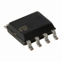
VNS3NV04D13TR STMicroelectronics, VNS3NV04D13TR Datasheet

VNS3NV04D13TR
Specifications of VNS3NV04D13TR
Available stocks
Related parts for VNS3NV04D13TR
VNS3NV04D13TR Summary of contents
Page 1
... COMPATIBLE WITH STANDARD POWER MOSFET DESCRIPTION The VNS3NV04D is a device formed by two monolithic OMNIFET II chips housed in a standard SO-8 package. The OMNIFET II are designed in STMicroelectronics VIPower M0-3 Technology: they are intended for replacement of standard Power MOSFETS from 50KHz BLOCK DIAGRAM INPUT1 GATE ...
Page 2
VNS3NV04D ABSOLUTE MAXIMUM RATING Symbol V Drain-source Voltage (V DSn V Input Voltage INn I Input Current INn R Minimum Input Series Impedance IN MINn I Drain Current Dn I Reverse DC Output Current Rn V Electrostatic Discharge (R=1.5K , ...
Page 3
THERMAL DATA Symbol R Thermal Resistance Junction-lead (per channel) thj-lead R Thermal Resistance Junction-ambient thj-amb When mounted on a standard single-sided FR4 board with 50mm (*) channel. ELECTRICAL CHARACTERISTICS (-40°C < T (Per each device) OFF Symbol Parameter Drain-source Clamp ...
Page 4
VNS3NV04D ELECTRICAL CHARACTERISTICS (continued) (T DYNAMIC Symbol Parameter Forward g (*) fs Transconductance C Output Capacitance OSS SWITCHING Symbol Parameter t Turn-on Delay Time d(on) t Rise Time r t Turn-off Delay Time d(off) t Fall Time f t Turn-on ...
Page 5
PROTECTION FEATURES During normal operation, the INPUT pin is electrically connected to the gate of the internal power MOSFET through a low impedance path. The device then behaves like a standard power MOSFET and can be used as a switch ...
Page 6
VNS3NV04D Fig.1: Switching Time Test Circuit for Resistive Load d(on) V gen Fig.2: Test Circuit for Diode Recovery Times I OMNIFET 220 6/ gen V gen 90 10% t ...
Page 7
Fig. 3: Unclamped Inductive Load Test Circuits R GEN Fig. 5: Input Charge Test Circuit Fig. 4: Unclamped Inductive Waveforms VNS3NV04D 7/14 1 ...
Page 8
VNS3NV04D Source-Drain Diode Forward Characteristics Vsd (mV) 1100 1050 Vin=0V 1000 950 900 850 800 750 700 650 600 (A) Derating Curve Static Drain-Source On resistance Vs. Input Voltage Rds(on) ...
Page 9
Static Drain-Source On Resistance Vs. Id Rds(on) (mohms) 250 225 Vin=5V 200 175 150 125 100 0.5 1 1.5 2 2.5 Id (A) Turn On Current Slope di/dt(A/us) 5 4.5 4 3.5 3 2.5 2 ...
Page 10
VNS3NV04D Turn Off Drain-Source Voltage Slope dv/dt(V/usec) 300 275 250 225 200 175 150 125 100 500 1000 1500 250 750 1250 Rg(ohm) Switching Time Resistive Load t(usec) 4 3.5 Vdd=15V 3 Id=1.5A Vin=5V 2.5 ...
Page 11
Normalized Input Threshold Temperature Vinth (V) 2 1.8 Vds=Vin 1.6 Id=1mA 1.4 1.2 1 0.8 0.6 0.4 0.2 0 -50 - 100 Tc (ºC) Step Response Current Limit Tdlim(usec) 13 12.5 12 11.5 11 10.5 10 ...
Page 12
VNS3NV04D DIM. MIN 0 0.65 b 0.35 b1 0. 4 3 12/14 SO-8 MECHANICAL DATA mm. TYP MAX. MIN. 1.75 0.25 0.003 1.65 ...
Page 13
B TAPE AND REEL SHIPMENT (suffix “13TR”) TAPE DIMENSIONS According to Electronic Industries Association (EIA) Standard 481 rev. A, Feb 1986 Tape width W Tape Hole Spacing P0 (± 0.1) Component Spacing P Hole Diameter D (± 0.1/-0) Hole Diameter ...
Page 14
... STMicroelectronics. Specifications mentioned in this publication are subject to change without notice. This publication supersedes and replaces all information previously supplied. STMicroelectronics products are not authorized for use as critical components in life support devices or systems without express written approval of STMicroelectronics. 2003 STMicroelectronics - Printed in ITALY- All Rights Reserved. ...


