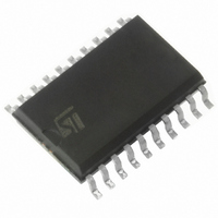
L9338DTR STMicroelectronics, L9338DTR Datasheet - Page 5

L9338DTR
Manufacturer Part Number
L9338DTR
Description
IC DRIVER QUAD LOW SIDE SOIC-20
Manufacturer
STMicroelectronics
Type
Low Sider
Datasheet
1.L9338MDTR.pdf
(8 pages)
Specifications of L9338DTR
Input Type
Inverting
Number Of Outputs
4
On-state Resistance
1.7 Ohm
Current - Peak Output
700mA
Voltage - Supply
4.5 V ~ 32 V
Mounting Type
Surface Mount
Package / Case
20-SOIC (7.5mm Width)
Switch Type
Low Side
Power Switch Family
L9338
Input Voltage
-24 to 45V
Power Switch On Resistance
1.7Ohm
Mounting
Surface Mount
Package Type
SO
Operating Temperature (min)
-40C
Operating Temperature (max)
150C
Operating Temperature Classification
Automotive
Pin Count
20
Lead Free Status / RoHS Status
Lead free / RoHS Compliant
Operating Temperature
-
Current - Output / Channel
-
Lead Free Status / Rohs Status
Compliant
Available stocks
Company
Part Number
Manufacturer
Quantity
Price
Company:
Part Number:
L9338DTR
Manufacturer:
IR
Quantity:
5 582
Part Number:
L9338DTR
Manufacturer:
ST
Quantity:
20 000
CIRCUIT DESCRIPTION
The L9838 is a quad low side driver for lines,
lamps or inductive loads in automotive and indus-
trial applications.
All INputs are TTL or CMOS compatible. This al-
lows the device to be driven directly by a micro-
controller. For the noise immunity, all inputs have
a Schmitt-trigger with a hysteresis of typ. 100mV.
Each input stage has an input voltage protection
from -24V to 45V. The device can be activated
with a ’high’ signal on ENable input. ENable ’low’
switches the device into the sleep mode. In this
mode the quiescent current is less than 10 A. A
high signal on PRoGramming input changes the
signal transfer polarity from noninverting into the
inverting mode. Normally this pin is connected to
V
nally fixed at low status by open input condition.
Independent of the PRoGramming input, the
OUTput switches off, if the signal INput pin is not
connected.
Each output driver has a current limitation of min
0.4A and a seperate thermal shut-down. The ther-
mal shut-down deactivates that output which ex-
DIAGNOSTIC TABLE
X = not relevant * selective for each channel at overtemperature
S
Normal function
Overtemperature,
disconnected ground or
supply voltage
Overtemperature
or GND. These pins (PRG and EN) are inter-
Pins
H
H
H
H
L
H
H
EN
L
L
H
H
X
L
H
PRG
ceeds Temperature switch off level. About 20K
below this temperature threshold the output will
be activated again. This means, that each output
is able to sink continuously 285mA without acti-
vating thermal shut-down at 85°C ambient tem-
perature (SO20). The slew rate of the output is
limited to max. 14V/ s to reduce the electromag-
netic interference, but not for the enable transfer
characteristic (see fig. 1). An integrated active fly-
back voltage limitation clamps the output voltage
during the flyback phase of inductive loads to typ.
50V. The power DMOS switches ON, if the device
is enabled and the OUTput swings below ground.
This protection avoids the activation of parasitics
inside the power DMOS.
The DIAGnostic is an open drain output. The logic
status depends on the PRoGramming pin. If the
PRG pin is ’low’ the DIAG output becomes low, if
the device works correctly.
At thermal shut-down of one channel, discon-
nected ground or supply voltage the DIAGnostic
output becomes high. If the PRG pin is ’high’ this
output is switched off at normal function and
switched on at overtemperature.
L
H
L
H
X
X
X
IN
L (on)
H (off)
H (off)
L (on)
H (off)
H (off) *
H (off) *
OUT
L (on)
L (on)
H(off)
H(off)
H(off)
H (off)
L (on)
DIAG
L9338
5/8


