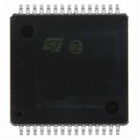
VND5004ASP30-E STMicroelectronics, VND5004ASP30-E Datasheet - Page 10

VND5004ASP30-E
Manufacturer Part Number
VND5004ASP30-E
Description
IC DRIVER HIGH SIDE 30-MPSO
Manufacturer
STMicroelectronics
Type
High Sider
Datasheet
1.VND5004ASP30TR-E.pdf
(34 pages)
Specifications of VND5004ASP30-E
Input Type
Non-Inverting
Number Of Outputs
2
On-state Resistance
4 mOhm
Current - Peak Output
100A
Voltage - Supply
4.5 V ~ 27 V
Operating Temperature
-40°C ~ 150°C
Mounting Type
Surface Mount
Package / Case
30-MPSO, MultiPowerSO
Product
Driver ICs - Various
Supply Voltage (min)
4.5 V
Supply Current
6 mA
Maximum Operating Temperature
+ 150 C
Mounting Style
SMD/SMT
Maximum Turn-off Delay Time
35000 ns
Maximum Turn-on Delay Time
25000 ns
Minimum Operating Temperature
- 40 C
Number Of Drivers
2
Device Type
High Side
Module Configuration
High Side
Peak Output Current
100A
Output Resistance
0.004ohm
Input Delay
25µs
Output Delay
35µs
Supply Voltage Range
4.5V To 27V
Rohs Compliant
Yes
Lead Free Status / RoHS Status
Lead free / RoHS Compliant
Current - Output / Channel
-
Lead Free Status / Rohs Status
Lead free / RoHS Compliant
Available stocks
Company
Part Number
Manufacturer
Quantity
Price
Electrical specifications
10/34
Table 8.
Table 9.
1. To ensure long term reliability under heavy overload or short circuit conditions, protection and related
Symbol
V
V
V
Symbol
T
V
T
DEMAG
V
CSD(hyst)
V
V
I
V
I(hyst)1,2
I
I
T
V
I
HYST
I
limH
limL
T
diagnostic signals must be used together with a proper software strategy. If the device is subjected to
abnormal conditions, this software must limit the duration and number of activation cycles.
I
CSDH
CSDL
TSD
IH1,2
ICL1,2
CSDH
IL1,2
CSDL
CSCL
RS
IH1,2
IL1,2
R
Short circuit current
Short circuit current
during thermal
cycling
Shutdown
temperature
Reset temperature
Thermal reset of
STATUS
Thermal hysteresis
(T
Turn-off output
voltage clamp
Input low level voltage
Low level input current
Input high level voltage
High level input current V
Input hysteresis
voltage
Input clamp voltage
CS_DIS low level
voltage
Low level CS_DIS
current
CS_DIS high level
voltage
High level CS_DIS
current
CS_DIS hysteresis
voltage
CS_DIS clamp voltage
TSD
Logic input
Protection and diagnostics
Parameter
-T
R
Parameter
)
V
5V<V
V
I
OUT
CC
CC
=13V
=13V; T
=2A; V
V
I
I
V
V
I
I
CC
IN
IN
CSD
CSD
IN
IN
CSD
CSD
Test conditions
=1mA
=-1mA
<24V
=0.9V
=2.1V
=1mA
=-1mA
=0.9V
=2.1V
IN
R
Test conditions
=0; L=6mH
<T
(1)
j
<T
TSD
VND5004A-E / VND5004ASP30-E
V
T
Min.
CC
150
RS
135
70
-27 V
+1
Min.
0.25
0.25
2.1
5.5
2.1
5.5
1
1
T
Typ.
CC
100
175
RS
40
7
-30 V
+5
Typ.
-0.7
-0.7
Max.
CC
140
140
200
Max.
-33
0.9
0.9
10
10
7
7
Unit
Unit
°C
°C
°C
°C
A
A
A
V
µA
µA
µA
µA
V
V
V
V
V
V
V
V
V
V


