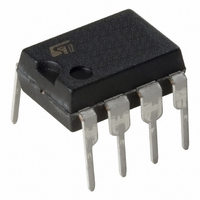
TDE1897CDP STMicroelectronics, TDE1897CDP Datasheet

TDE1897CDP
Specifications of TDE1897CDP
TDE1897CDP
Available stocks
Related parts for TDE1897CDP
TDE1897CDP Summary of contents
Page 1
... TDE1897C TDE1898C 0.5A HIGH-SIDE DRIVER MULTIPOWER BCD TECHNOLOGY Minidip SIP9 ORDERING NUMBERS: TDE1897CDP TDE1898CSP TDE1898CDP ogy, for driving inductive or resistive loads. An in- ternal Clamping Diode enables the fast demag- netization of inductive loads. Diagnostic for CPU feedback and extensive use of electrical protections make this device inher- ently indistructible and suitable for general pur- pose industrial applications ...
Page 2
TDE1897C - TDE1898C PIN CONNECTIONS (Top view) Minidip SIP9 ABSOLUTE MAXIMUM RATINGS (Minidip pin reference) Symbol V Supply Voltage (Pins – V Supply to Output Differential Voltage. See also Input ...
Page 3
ELECTRICAL CHARACTERISTICS (V Symbol Parameter V 3 Supply Voltage for Valid smin Diagnostics V 3 Supply Voltage (operative Quiescent Current out os V Undervoltage Threshold 1 sth1 V 3 Undervoltage Threshold ...
Page 4
TDE1897C - TDE1898C SOURCE DRAIN NDMOS DIODE Symbol Parameter V 2-3 Forward On Voltage fsd I 2-3 Forward Peak Current fp t 2-3 Reverse Recovery Time rr t 2-3 Forward Recovery Time fr THERMAL CHARACTERISTICS (*) Lim Junction Temp. Protect. ...
Page 5
APPLICATION INFORMATION DEMAGNETIZATION OF INDUCTIVE LOADS An internal zener diode, limiting the voltage across the Power MOS to between 45 and 55V (V ), provides safe and fast demagnetization of cl inductive loads without external clamping devices. The maximum energy ...
Page 6
TDE1897C - TDE1898C WORST CONDITION POWER DISSIPATION IN THE ON-STATE In IPS applications the maximum average power dissipation occurs when the device stays for a long time in the ON state. In such a situation the internal temperature depends on ...
Page 7
All electrical parameters of the device, con- cerning the calculation, are at maximum val- ues. - Thermal shutdown threshold is at minimum value heat sink nor air circulation ( thj-amb Therefore: ...
Page 8
TDE1897C - TDE1898C Figure 6: Max. Output Current vs. Ambient Temperature (Minidip Package 100 C/W) th j-amb (mA) 600 500 400 300 200 100 Figure 8: Max. Output Current vs. Ambient Temperature (SIP9 ...
Page 9
DIM. MIN. TYP. MAX. MIN. A 3.32 a1 0.51 0.020 B 1.15 1.65 0.045 b 0.356 0.55 0.014 b1 0.204 0.304 0.008 D 10.92 E 7.95 9.75 0.313 e 2.54 e3 7.62 e4 7.62 F 6.6 I 5.08 L ...
Page 10
TDE1897C - TDE1898C mm DIM. MIN. TYP. MAX. A 7.1 a1 2.7 3 0.106 24.8 b1 0.5 b3 0.85 1.6 0.033 C 3.3 c1 0.43 c2 1.32 D 21.2 d1 14.5 e 2.54 e3 20.32 L 3.1 ...
Page 11
DIM. MIN. TYP. MAX. MIN. A 2.35 2.65 0.093 A1 0.1 0.3 0.004 B 0.33 0.51 0.013 C 0.23 0.32 0.009 D 12.6 13 0.496 E 7.4 7.6 0.291 e 1. 10.65 0.394 h 0.25 0.75 0.010 ...
Page 12
... STMicroelectronics. Specifications mentioned in this publication are subject to change without notice. This publication supersedes and replaces all information previously supplied. STMicroelectronics products are not authorized for use as critical components in life support devices or systems without express written approval of STMicroelectronics. The ST logo is a registered trademark of STMicroelectronics. ...


