VN770P13TR STMicroelectronics, VN770P13TR Datasheet
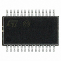
IC RELAY SSR QUAD SMART 28-SSOP

VN770P13TR

Manufacturer Part Number
VN770P13TR
Description
IC RELAY SSR QUAD SMART 28-SSOP
Manufacturer
STMicroelectronics
Type
H Bridger
Datasheet

Specifications of VN770P13TR

Input Type
Non-Inverting
Number Of Outputs
4
On-state Resistance
160 mOhm
Current - Output / Channel
9A
Voltage - Supply
5.5 V ~ 36 V
Operating Temperature
-40°C ~ 150°C
Mounting Type
Surface Mount
Package / Case
28-SOIC (7.5mm Width)
Supply Current
4 mA
Maximum Operating Temperature
85 C
Mounting Style
SMD/SMT
Minimum Operating Temperature
- 40 C
Lead Free Status / RoHS Status
Lead free / RoHS Compliant
Current - Peak Output
-
Lead Free Status / Rohs Status
Lead free / RoHS Compliant
* Total resistance of one side in bridge configuration
DESCRIPTION
The VN770P is a device formed by three
monolithic chips housed in a standard SO28
package: a double high side and two low side
switches. Both the double high side and low side
switches are made using STMicroelectronics
VIPower technology. This device is suitable to
drive a DC motor in a bridge configuration as well
as to be used as a quad switch for any low
voltage application. The dual high side switches
have built-in thermal shut-down to protect the
chip from over temperature and short circuit,
status output to provide indication for open load
in off and on state, overtemperature conditions
and stuck-on to V
two OMNIFET types (fully autoprotected Power
MOSFET in VIPower
built-in thermal shut-down, linear current limitation
and overvoltage clamping. Fault feedback for
thermal
monitoring the voltage at the input pin.
DUAL HIGH-SIDE SWITCH
From the falling edge of the input signal, the
status output, initially low
condition
on-state), will go back to a high state with a
different delay in case of overtemperature (tpovl)
and in case of open open load (
This feature allows to discriminate the nature of
the detected fault. To protect the device against
September 1998
VN770P
IDEAL AS A LOW VOLTAGE BRIDGE
LINEAR CURRENT LIMITATION
VERY LOW STAND-BY POWER
DISSIPATION
SHORT CIRCUIT PROTECTED
STATUS FLAG DIAGNOSTICS
OPEN DRAIN DIAGNOSTICS OUTPUT
INTEGRATED CLAMPING CIRCUITS
UNDER-VOLTAGE PROTECTION
ESD PROTECTION
T YPE
intervention
(overtemperature
R
0.270
DS( on)
FOR COMPLETE H BRIDGE CONFIGURATIONS
CC
*
. The low side switches are
QUAD SMART POWER SOLID STATE RELAY
can
technology). They have
I
9 A
OUT
be
to signal a fault
or
tpol
) respectively.
detected
open
26 V
V
CC
load
by
short circuit and over current condition, the
thermal protection turns the integrated Power
MOS off at a minimum junction temperature of
140
the switch is automatically turned on again. In
short circuit the protection reacts with virtually no
delay, the sensor (one for each channel) being
located inside each of the two Power MOS areas.
This positioning allows the device to operate with
one channel in automatic thermal cycling and the
other one on a normal load. An internal function
of the devices ensures the fast demagnetization
of inductive loads with a typical voltage (V
of -18V. This function allows to greatly reduces
the power dissipation according to the formula:
P
where f = switching frequency and
V
In this device if the GND pin is disconnected, with
V
off.
LOW-SIDE SWITCHES
During normal operation, the Input pin is
electrically connected to the gate of the internal
power MOSFET. The device then behaves like a
standard power MOSFET and can be used as a
switch from DC to 50 KHz. The only difference
from the user’s standpoint is that a small DC
current (I
supply the internal circuitry.
dem
demag
CC
o
not exceeding 16V, both channel will switch
= 0.5 L
C. When this temperature returns to 125
= demagnetization voltage.
iss
) flows into the Input pin in order to
load
(I
load
)
SO-28
2
[(V
CC
+V
VN770P
demag
)/V
demag
demag
] f
1/11
o
C
)

Related parts for VN770P13TR

VN770P13TR Summary of contents

Page 1

... SO28 package: a double high side and two low side switches. Both the double high side and low side switches are made using STMicroelectronics VIPower technology. This device is suitable to drive a DC motor in a bridge configuration as well used as a quad switch for any low voltage application ...

Page 2

VN770P BLOCK DIAGRAM 2/11 ...

Page 3

CONNECTION DIAGRAM PIN FUNCTION No NAME 1, 3, 25, 28 DRAIN 3 Drain of Switch 3 (low-side switch) 2 INPUT 3 Input of Switch 3 (low-side switch N.C. Not Connected 5, 10, 19 Drain of Switches ...

Page 4

VN770P PROTECTION CIRCUITS DUAL HIGH SIDE SWITCH The simplest way to protect the device against a continuous reverse battery voltage (-26V insert a a small resistor between pin 2 (GND) and ground. The suggested resistance value is about ...

Page 5

ABSOLUTE MAXIMUM RATING (-40 HIGH SIDE SWITCH Symbol V Drain-Source Breakdown Voltage (BR)DSS I Output Current (cont. ) OUT I Reverse O utput Current R I Input Current Reverse Supply Voltage atus Current STAT ...

Page 6

VN770P ELECTRICAL CHARACTERISTICS FOR DUAL HIGH SIDE SWITCH (continued) R Output internal i Im pedance SWITCHING Symbol Parameter t (^) Turn-on Delay Time Of d(on) Output Current t (^) Rise Time Of O utput r Current t ...

Page 7

ELECTRICAL CHARACTERISTICS FOR DUAL HIGH SIDE SWITCH (continued) PROTECTION AND DIAGNOSTICS Symbol Parameter I Open Load Current OL Level t St atus Delay povl t St atus Delay pol (*) In= Nominal current according to ISO definition for high side ...

Page 8

VN770P ELECTRICAL CHARACTERISTICS FOR LOW SIDE SWITCHES (continued Forward fs Transconductance C Output Capacitance os s SWITCHING (**) Symbol Parameter t Turn-on Delay Time d Rise Time r t Turn-off Delay Time d ...

Page 9

TYPICAL APPLICATION DIAGRAM VN770P 9/11 ...

Page 10

VN770P SO-28 MECHANICAL DATA DIM. MIN. TYP 0.10 b 0.35 b1 0. 17.7 E 10.00 e 1.27 e3 16.51 F 7.40 L 0.40 S 10/11 mm MAX. MIN. 2.65 0.30 0.004 0.49 0.013 0.32 ...

Page 11

... STMicroelectronics. Specification mentioned in this publication are subject to change without notice. This publication supersedes and replaces all information previously supplied. STMicroelectronics products are not authorized for use as critical components in life support devices or systems without express written approval of STMicroelectronics. The ST logo is a registered trademark of STMicroelectronics 1998 STMicroelectronics – ...

Related keywords