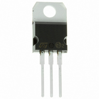
VNP14N04-E STMicroelectronics, VNP14N04-E Datasheet

VNP14N04-E
Specifications of VNP14N04-E
Available stocks
Related parts for VNP14N04-E
VNP14N04-E Summary of contents
Page 1
... DIRECT ACCESS TO THE GATE OF THE POWER MOSFET (ANALOG DRIVING) COMPATIBLE WITH STANDARD POWER MOSFET STANDARD TO-220 PACKAGE DESCRIPTION The VNP14N04 is a monolithic device made using STMicroelectronics VIPower Technology, Technology, intended for replacement standard power MOSFETS KHz applications. Built-in thermal shut-down, linear ...
Page 2
... VNP14N04 ABSOLUTE MAXIMUM RATING Symbol Parameter V Drain-source Voltage ( Input Voltage in I Drain Current D I Reverse DC Output Current R V Electrostatic Discharge (C= 100 pF, R=1 esd P Total Dissipation at T tot T Operating Junction Temperature j T Case Operating Temperature c T Storage Temperature stg THERMAL DATA R Thermal Resistance Junction-case ...
Page 3
... DD j (see test circuit, figure 5) Test Conditions starting gen VNP14N04 Min. Typ. Max. Unit 60 120 ns 160 300 ns 250 400 ns 100 200 ns 300 500 ns 1.5 2.2 s 5.5 7.5 s 1.8 2.5 s 120 Min. Typ. Max. Unit 1.6 V 110 ns 0.34 C 6.1 A Min. Typ. Max. ...
Page 4
... VNP14N04 PROTECTION FEATURES During normal operation, the Input pin is electrically connected to the gate of the internal power MOSFET. The device then behaves like a standard power MOSFET and can be used as a switch from KHz. The only difference from the user’s standpoint is that a small DC ...
Page 5
... Thermal Impedance Output Characteristics Static Drain-Source On Resistance vs Input Voltage Derating Curve Transconductance Static Drain-Source On Resistance VNP14N04 5/11 ...
Page 6
... VNP14N04 Static Drain-Source On Resistance Capacitance Variations Normalized On Resistance vs Temperature 6/11 Input Charge vs Input Voltage Normalized Input Threshold Voltage vs Temperature Normalized On Resistance vs Temperature ...
Page 7
... Turn-on Current Slope Turn-off Drain-Source Voltage Slope Switching Time Resistive Load Turn-on Current Slope Turn-off Drain-Source Voltage Slope Switching Time Resistive Load VNP14N04 7/11 ...
Page 8
... VNP14N04 Switching Time Resistive Load Step Response Current Limit 8/11 Current Limit vs Junction Temperature Source Drain Diode Forward Characteristics ...
Page 9
... Fig. 1: Unclamped Inductive Load Test Circuits Fig. 3: Switching Times Test Circuits For Resistive Load Fig. 5: Test Circuit For Inductive Load Switching And Diode Recovery Times Fig. 2: Unclamped Inductive Waveforms Fig. 4: Input Charge Test Circuit Fig. 6: Waveforms VNP14N04 9/11 ...
Page 10
... VNP14N04 DIM L20 L30 P Q Package Weight 10/11 TO-220 MECHANICAL DATA mm. MIN. TYP 4.40 0.61 1.15 0.49 15.25 10 2.40 4.95 1.23 6.20 2.40 13 3.50 16.40 28.90 3.75 2.65 1.9Gr. (Typ.) MAX. 4.60 0.88 1.70 0.70 15.75 10.40 2.70 5.15 1.32 6.60 2 ...
Page 11
... STMicroelectronics - Printed in ITALY- All Rights Reserved. Australia - Brazil - Canada - China - Finland - France - Germany - Hong Kong - India - Israel - Italy - Japan - Malaysia - Malta - Morocco - Singapore - Spain - Sweden - Switzerland - United Kingdom - U.S.A. The ST logo is a trademark of STMicroelectronics STMicroelectronics GROUP OF COMPANIES http://www.st.com VNP14N04 11/11 ...


