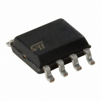
L6560AD STMicroelectronics, L6560AD Datasheet - Page 4

L6560AD
Manufacturer Part Number
L6560AD
Description
IC PWR FACTOR CORRECTOR 8 SOIC
Manufacturer
STMicroelectronics
Datasheet
1.L6560AD.pdf
(11 pages)
Specifications of L6560AD
Mode
Discontinuous (Transition)
Current - Startup
300µA
Voltage - Supply
11 V ~ 18 V
Operating Temperature
-20°C ~ 150°C
Mounting Type
Surface Mount
Package / Case
8-SOIC (3.9mm Width)
Maximum Operating Temperature
+ 150 C
Mounting Style
SMD/SMT
Minimum Operating Temperature
- 25 C
Lead Free Status / RoHS Status
Contains lead / RoHS non-compliant
Frequency - Switching
-
Lead Free Status / Rohs Status
Lead free / RoHS Compliant
Other names
497-1438-5
Available stocks
Company
Part Number
Manufacturer
Quantity
Price
Part Number:
L6560AD013TR
Manufacturer:
ST
Quantity:
20 000
L6560 - L6560A
ELECTRICAL CHARACTERISTICS (continued)
ZERO CURRENT DETECTOR
OUTPUT SECTION
OUTPUT OVERVOLTAGE SECTION
RESTART TIMER
OVER VOLTAGE PROTECTION OVP
The output voltage is expected to be kept by the
operation of the PFC circuits close to its reference
value that is set by the ratio of the two external re-
sistors R
eration that the non inverting input of the error
amplifier is biased inside the L6560 at 2.5V.
In steady state conditions, the current through R1
and R2 is:
and, if the external compensation network is
made only with a capacitor C, the current through
C is equal zero.
When the output voltage increases abruptly the
current through R1 becomes:
4/11
Symbol
Symbol
Symbol
Symbol
t
V
V
V
START
V
I
OVP
ZCD
ZCD
ZCD
t
GD
t
r
f
1
and R
Pin
Pin
Pin
Pin
5
5
5
7
7
7
2
I
SC
I
2
R1
Input Threshold Voltage Rising
Edge
Hysteresis
Clamp Voltage
Clamp Voltage
Dropout Voltage
Output Voltage Rise Time
Output Voltage Fall Time
OVP Triggering Current
Start Timer
(see fig. 2), taking into consid-
or I
V
V
SC
outsc
out
R1
R1
Parameter
Parameter
Parameter
Parameter
2.5
R2
2.5
2.5
I
I
I
I
I
I
CL = 1nF
CL = 1nF
ZCD
ZCD
GDsource
GDsource
GDsink
GDsink
= 3mA
= –3mA
= 200mA
= 20mA
Test Condition
Test Condition
Test Condition
Test Condition
Since the current through R2 doesn’t change, the
enter in the error amplifier.
This current is mirrored inside the L6560, and
compared with a precise internal reference of
40 A. Whenever such 40 A limit is exceed, the
OVP protection is triggered (Dynamic OVP), and
the external power transistor is switched off, until
the overvoltage situation disappears. However if
the overvoltage persists, before that the transient
condition of dynamic circuit exhausts, an internal
comparator (Static OVP) latches the OVP condi-
tion keeping the external power switch turned off
(see fig. 1).
The OVP value is threfore set by the equation
OVP = Vout = R
Typical values for R
the application circuit. The overvoltage can be set
independently from the average output voltage.
The precision in setting the overvoltage threshold
is 7% of the overvoltage value (for instance V =
60V
= 200mA
= 20mA
I current must flow through the capacitor C and
4.2V).
I
R1
V
outsc
1
40 A.
1
R1
, R
V
Min.
Min.
Min.
Min.
1.8
0.3
0.4
36
45
OUT
5
2
and C are reported in
2.5
Typ.
Typ.
Typ.
Typ.
0.5
5.7
0.7
1.2
0.7
50
40
40
60
I
sc
Max.
Max.
Max.
Max.
120
100
2.3
0.7
6.4
1.5
0.3
44
1
2
1
I.
Unit
Unit
Unit
Unit
ns
ns
V
V
V
V
V
V
V
V
A
s


