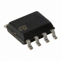
E-L6561D STMicroelectronics, E-L6561D Datasheet - Page 2

E-L6561D
Manufacturer Part Number
E-L6561D
Description
IC POWER FACTOR CORRECTOR 8-SOIC
Manufacturer
STMicroelectronics
Datasheet
1.L6561D013TR.pdf
(13 pages)
Specifications of E-L6561D
Mode
Discontinuous (Transition)
Current - Startup
50µA
Voltage - Supply
11 V ~ 18 V
Operating Temperature
-25°C ~ 125°C
Mounting Type
Surface Mount
Package / Case
8-SOIC (3.9mm Width)
Start-up Supply Current
50uA
Operating Supply Voltage (min)
11V
Operating Supply Voltage (max)
18V
Operating Temp Range
-40C to 150C
Operating Temperature Classification
Automotive
Package Type
SOIC
Pin Count
8
Mounting
Surface Mount
Maximum Operating Temperature
+ 150 C
Mounting Style
SMD/SMT
Minimum Operating Temperature
- 40 C
Lead Free Status / RoHS Status
Lead free / RoHS Compliant
Frequency - Switching
-
Lead Free Status / Rohs Status
Compliant
Other names
497-4581-5
Available stocks
Company
Part Number
Manufacturer
Quantity
Price
L6561
Table 2. Absolute Maximum Ratings
Figure 3. Pin Connection (Top view)
Table 3. Thermal Data
Table 4. Pin Description
(1) Parameter guaranteed by design, not tested in production.
2/13
INV, COMP
Symbol
R
Symbol
th j-amb
MULT
N.
ZCD
1
2
3
4
5
6
7
8
T
I
P
I
CS
Vcc
GD
T
stg
tot
j
Thermal Resistance Junction to ambient
COMP
Name
MULT
GND
ZCD
INV
V
GD
CS
1, 2, 3
CC
Pin
8
7
4
5
Inverting input of the error amplifier. A resistive divider is connected between the output
regulated voltage and this point, to provide voltage feedback.
Output of error amplifier. A feedback compensation network is placed between this pin and the
INV pin.
Input of the multiplier stage. A resistive divider connects to this pin the rectified mains. A voltage
signal, proportional to the rectified mains, appears on this pin.
Input to the comparator of the control loop. The current is sensed by a resistor and the resulting
voltage is applied to this pin.
Zero current detection input. If it is connected to GND, the device is disabled.
Current return for driver and control circuits.
Gate driver output. A push pull output stage is able to drive the Power MOS with peak current of
400mA (source and sink).
Supply voltage of driver and control circuits.
I
Output Totem Pole Peak Current (2 s)
Analog Inputs & Outputs
Current Sense Input
Zero Current Detector
Power Dissipation @T
Junction Temperature Operating Range
Storage Temperature
q
+ I
Z
; (I
GD
= 0)
COMP
MULT
INV
Parameter
CS
amb
Parameter
= 50 °C
1
2
3
4
DIP8
Function
8
7
6
5
(DIP-8)
(SO-8)
V
GD
GND
ZCD
CC
SO 8
150
50 (source)
-40 to 150
-55 to 150
-10 (sink)
-0.3 to 7
-0.3 to 7
Value
±700
0.65
30
1
MINIDIP
100
°C/W
Unit
Unit
mA
mA
mA
mA
°C
°C
W
W
V
V


