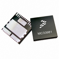
MC33981BPNA Freescale Semiconductor, MC33981BPNA Datasheet - Page 24

MC33981BPNA
Manufacturer Part Number
MC33981BPNA
Description
IC SWITCH HI SIDE SINGLE 16-PQFN
Manufacturer
Freescale Semiconductor
Type
High Side Switchr
Datasheet
1.MC33981BPNA.pdf
(37 pages)
Specifications of MC33981BPNA
Number Of Outputs
1
Rds (on)
4 mOhms
Internal Switch(s)
Yes
Current Limit
40A
Voltage - Input
6 ~ 27 V
Operating Temperature
-40°C ~ 125°C
Mounting Type
Surface Mount
Package / Case
16-PQFN, 16-PowerQFN
Lead Free Status / RoHS Status
Contains lead / RoHS non-compliant
Available stocks
Company
Part Number
Manufacturer
Quantity
Price
Part Number:
MC33981BPNA
Manufacturer:
FREESCALE
Quantity:
20 000
EMC RESULTS AND IMPROVEMENTS
+ 1.0mH) switching at 20 kHz with duty = 80%. The current in
the load was 17 A continuous.
BOARD SETUP
in
24
33981
TYPICAL APPLICATIONS
EMC AND EMI RECOMMENDATIONS
Key
1
2
3
4
5
6
7
Figure
The 33981 OUT is connected to an inductive load (0.47 Ω
The initial configuration of our 33981 board is represented
EUT (grounded locally if
required in test plan)
Test harness
Load simulator (placement
and ground connection)
Power supply (location
optional)
Artificial Network (AN)
Ground plane (bonded to
shielded enclosure)
Low relative permittivity
support (
Figure 24. Test Bench for Radiated Emission
25.
ερ
≤ 1.4)
10 High quality double-
11 Bulkhead connector
12 Measuring instrument
13 RF absorber material
14 Stimulation and monitoring
8
–
Biconical antenna
–
shielded coaxial cable
(50 Ω)
system
switching times are the maximum values. A capacitor of
1000 μF is connected between VPWR and GND.
CONDUCTED MEASUREMENTS
TEST SETUP
accordance with the CISPR 25 standard, the test bench in
Figure 26, Conducted Emission Test Setup, on page 24
developed.
EFFECTS OF SOME PARAMETERS
When the duty increases the di/dt on the VPWR line is higher.
The device has to deliver more current and provide more
energy.
on the V
level rises with the output frequency. This is due to the
increasing number of commutations.
No SR capacitor is used. Therefore, the obtained
To perform a conducted emission measurement in
The conducted emissions level rise with the duty cycle.
Figure 26. Conducted Emission Test Setup
Figure 27
PWR
Figure 25.
33981
current waveform. The conducted emission
describes the effect of duty cycle increase
33981
Analog Integrated Circuit Device Data
Initial Configuration
Out
Freescale Semiconductor
V
PWR
Power Supply
LISN
Measurement
Point for
Conducted
Emission
EUT
Non-Conductive
Material
Load (1.0 mH + 0.47 Ω)
Optical PWM Signal
GND
was


