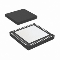
LP3913SQ-ADJ/NOPB National Semiconductor, LP3913SQ-ADJ/NOPB Datasheet - Page 27

LP3913SQ-ADJ/NOPB
Manufacturer Part Number
LP3913SQ-ADJ/NOPB
Description
IC POWER MANAGEMENT 48-LLP
Manufacturer
National Semiconductor
Series
PowerWise®r
Datasheet
1.LP3913SQ-ACNOPB.pdf
(58 pages)
Specifications of LP3913SQ-ADJ/NOPB
Applications
Handheld/Mobile Devices
Voltage - Supply
2.5 V ~ 6 V
Operating Temperature
-40°C ~ 85°C
Mounting Type
Surface Mount
Package / Case
48-LLP
Lead Free Status / RoHS Status
Lead free / RoHS Compliant
Current - Supply
-
Other names
LP3913SQ-ADJ
LP3913SQ-ADJ
LP3913SQ-ADJTR
LP3913SQ-ADJ
LP3913SQ-ADJTR
Symbol
T1
T2
T3
T4
T5
Symbol
T1
T2
T3
T4
T5
Power On Timing
Each timeout T1 thru to T5 are factory programmed from 0 ms to 63 ms. The following defaults are shown below.
Power Off Timing
The timing delays during a power off sequence are equal to 63 ms minus the timing delay during the power on sequence.
Transitioning from Standby to Active Mode (Power Up)
Battery Power Present Only
When only battery power is present and the battery voltage
V
wakeup signals. The first is the ONOFF pin. The second and
third wakeups are the Wall Adapter and USBPWR. The
ONOFF pin is factory programmable wakeup source. It can
be a rising edge, a falling edge, a level high, or a level low
event. Regardless of the mode, the signal requires a 32 ms
deglitch time. A deglitched version of the ONOFF pin is output
on the open-drain output pin ONSTAT. ONOFF is usually
connected to a push button. Asserting the ONOFF pin starts
the power on sequencer. This enables the DC/DC converters
BATT
> V
BATTLOW
, the LP3913 is waiting for one of three valid
Description
Programmable Delay for LDO1 and LDO2
Programmable Delay to Buck1
Programmable Delay for Buck2
Programmable Delay for Buck3
Programmable Delay for NRST
Description
Programmable delay for LDO1 and LDO2
Programmable delay to Buck1
Programmable delay for Buck2
Programmable delay for Buck3
Programmable delay for NRST
Power up sequence:
27
including the Buck1 DC/DC converter that supplies power to
the system processor. The system processor then needs to
set bit D4 (PACK bit) in the Power On Event Register through
the I
to keep the LP3913 in the Active mode. These serve as a
Power Acknowledgement, confirming the power on request
initiated by the ONOFF pin. If neither the PACK bit (D4) in the
PON register or the POWERACK pin is set within 128 ms
(max) of the start of the power-up sequencer, then the LP3913
will automatically turn off, as the system failed to acknowledge
the power on request. Connecting the battery will be consid-
ered a Power on event. However hot insertion of the battery
with the adapter connected is NOT permitted.
2
C interface or apply a logic high to the POWERACK pin
30000105
Time
Time
15
20
25
60
58
48
43
38
5
3
www.national.com
Units
Units
ms
ms
ms
ms
ms
ms
ms
ms
ms
ms


