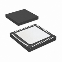
LP3913SQ-ADJ/NOPB National Semiconductor, LP3913SQ-ADJ/NOPB Datasheet - Page 39

LP3913SQ-ADJ/NOPB
Manufacturer Part Number
LP3913SQ-ADJ/NOPB
Description
IC POWER MANAGEMENT 48-LLP
Manufacturer
National Semiconductor
Series
PowerWise®r
Datasheet
1.LP3913SQ-ACNOPB.pdf
(58 pages)
Specifications of LP3913SQ-ADJ/NOPB
Applications
Handheld/Mobile Devices
Voltage - Supply
2.5 V ~ 6 V
Operating Temperature
-40°C ~ 85°C
Mounting Type
Surface Mount
Package / Case
48-LLP
Lead Free Status / RoHS Status
Lead free / RoHS Compliant
Current - Supply
-
Other names
LP3913SQ-ADJ
LP3913SQ-ADJ
LP3913SQ-ADJTR
LP3913SQ-ADJ
LP3913SQ-ADJTR
ANALOG TO DIGITAL CONVERTER
LP3913 is equipped with an 8-bit dual-slope integrating ana-
log to digital converter. Dual-slope converters provide effec-
tive filtering of >500 kHz and <125 kHz noise components on
the input voltage, and does not require a sample and hold
stage. The A/D converter core digitizes the input voltage
ranging from V
The A/D converter multiplexes 4 different sources:
1.
2.
3.
4.
The voltage ranges for the first two sources are scaled to
match the input voltage interval of the A/D converter: [V
2V
Battery Voltage Measurement
The battery voltage scalar transforms the battery voltage
ranging from 2.6V–3.5V to the reference voltage interval:
[V
selected through I
register 0xA to 0’b1.
Battery Charge Current Measurement
The battery charge current is indirectly measured by measur-
ing the voltage across the I
the battery charge current is mirrored over the I
and hence:
where K is a ratio between the R
current.
The battery charge current scalar transforms the voltage
across the external I
put voltage interval of the A/D converter.
REFH
REFH
The battery voltage
The battery charge current
External source ADC1
External source ADC2
, 2*V
]. This is accomplished by using two internal scalars.
REFH
REF
]. A wider voltage range (2.6V–4.4V) can be
2
to 2V
C by setting the voltage range bit D7 in
V
SENSE
ISENSE
REF
resistor to the [V
, where V
= K * I
SENSE
SENSE
CHARGE
resistor. A fixed portion of
REF
current and the charge
is the voltage mea-
REFH
SENSE
, 2*V
Simplified ADC Block Diagram
REFH
resistor
REFH
] in-
,
39
sured on the V
first activation of the ADC enable bit, the dual-slope converter
integrates the input signal during the first phase for approxi-
mately 2 ms, followed by a second phase that integrates
V
signal. As a result the total conversion time varies from 2 ms
to 4 ms.
External General Purpose Sources
Two additional A/D converter sources are available on the
ADC1 and ADC2 pins of the LP3913. These two external A/
D converter sources are not internally scaled and have an
input voltage range of [V
can use these two sources for general purpose applications
such as resistive keyboard matrix scanning, temperature
measurements, battery load current, battery ID resistor mea-
surement, etc.
REF
for 0 ms to 2 ms depending on the level of the input
REFH
pin. After an initial 2 ms warm-up for the
REFH
, 2*V
REFH
]. The system designer
30000120
www.national.com
30000121


