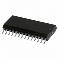
SA5778D,518 NXP Semiconductors, SA5778D,518 Datasheet - Page 10

SA5778D,518
Manufacturer Part Number
SA5778D,518
Description
IC SERIAL TRPL GAUGE DRVR 28SOIC
Manufacturer
NXP Semiconductors
Datasheet
1.SA5778DCE1804512.pdf
(16 pages)
Specifications of SA5778D,518
Applications
Automotive
Current - Supply
500µA
Voltage - Supply
8 V ~ 16 V
Operating Temperature
-40°C ~ 105°C
Mounting Type
Surface Mount
Package / Case
28-SOIC (7.5mm Width)
Lead Free Status / RoHS Status
Lead free / RoHS Compliant
Other names
935260762518
SA5778D-T
SA5778D-T
SA5778D-T
SA5778D-T
Philips Semiconductors
Sample Calculations for Power Dissipation and
Thermal Management
Worst Case Example
The worst case example will occur when the STGD is operating at
V
(105 C), and with the lowest specified coil resistance (171 ohms at
25 C). Typical coil self heating of 15 C is assumed.
Calculation of Coil resistance operating at 105 C ambient.
Calculation of STGD power dissipation at 16 volt operation.
Required board area and Junction Temperature calculation
The maximum junction temperature desired is 150 C. The
permissible temperature rise and required
as:
Where; T = Temperature rise in C
1998 Apr 03
BATTMAX
Serial triple gauge driver (STGD)
R
P
P
T
T
amb
CA
T = T
j
T = T
D
D
JA
JA
= Junction Temperature
= 171 x(1+(0.4%((15+105)–25)))
= 236 Ohms at T
= V
+V
= 16(16/236)+16(0.012)+1.5(16–1.5–0.5)/320
= 1.085+0.192+0.066 Watts
= 1.34 Watts
= Power dissipation
= R
= T/P
= T/P
= Ambient Temperature
OL2
j
J
BATT
–T
(16V, in the highest specified ambient temperature
CN
DATA
–T
DATA
S
amb
CS
amb
(V
(1+(0.4%W/ C)*((T
CLK
D
D
OUT
(V
BATT
IN
=55 C/1.34 watts = 33 C/W.
BATT
= 150 – 105 = 45 C
– V
/R
amb
C
OL2
) + V
=105 C, with 15 C of self heating.
– V
t
CSH
BATT
t
SU
BE(PNP)
SH
+T
D29
S4
(0.012)
amb
) / R
)–25 C))
1
L
JA
may be calculated
t
t
DR
CF
Figure 10. Serial Interface Timing
t
CR
D1*
D1
t
HD
10
30 CLOCK CYCLES
29
From Figure 8, the copper area required, using a single sided board,
to keep the junction temperature within limits is approximately
2200 mm
double-sided board.
The above example illustrates the worst case situation of the STGD
operating in at a maximum battery voltage, with the lowest nominal
coil resistance (171 at room temperature), and at the highest
ambient temperature. This will produce the highest junction
temperature. At lower ambient temperatures the power dissipation
may be higher because the coil resistance is decreased, however
the junction temperature will be lower.
Serial Interface
Figure 10 demonstrates the serial interface timing referenced in the
AC specifications. Figure 11 shows the order of information transfer
through the serial interface. On a low to high transition of the CS pin,
status information replaces the four most significant bits of data in
the shift register and are the first bits shifted out. Output data is
changed on the falling edge of S
the rising edge of S
with the most significant bit, followed by minor gauge 1 data then
minor gauge 2 data.
t
DF
t
CYC
2
. Figure 9 shows 1200 mm
t
SCLKL
D0*
D0*
CLK
. Major gauge data is loaded first, starting
t
SCLKH
30
CLK
, while input data is captured on
2
is required on each side of a
t
CSL
Product specification
SA5778
SR01499


