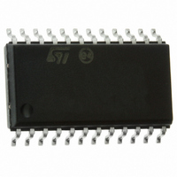
L6610D STMicroelectronics, L6610D Datasheet - Page 4

L6610D
Manufacturer Part Number
L6610D
Description
IC CTRLR HOUSEKEEPING BCD 24SOIC
Manufacturer
STMicroelectronics
Datasheet
1.L6610DTR.pdf
(29 pages)
Specifications of L6610D
Applications
Programmable Housekeeping Controller
Voltage - Supply
4.2 V ~ 7 V
Current - Supply
5mA
Operating Temperature
0°C ~ 105°C
Mounting Type
Surface Mount
Package / Case
24-SOIC (7.5mm Width)
Lead Free Status / RoHS Status
Lead free / RoHS Compliant
Voltage - Input
-
Available stocks
Company
Part Number
Manufacturer
Quantity
Price
Part Number:
L6610D
Manufacturer:
ST
Quantity:
20 000
PIN DESCRIPTION (continued)
L6610
4/29
Pin #
10
11
12
13
14
15
16
4
5
6
7
8
9
12Visns
3V3isns
DFAULT
PS-ON /
5Visns/
PW-OK
ACsns
Dmon
Name
Clock
VREF
/Data
Aout
Cout
Ainv
Cinv
Vdd
Output of the error amplifier for the main converter. This pin typically drives an optocoupler and is
also used for compensation along with Ainv (pin #5).
Main loop error amplifier inverting input. The non-inverting input is connected to an internal 2.5V
reference that can be digitally trimmed. A high impedance internal divider from +12V and +5V
UV/OV sense pins (#23, #24) eliminates the need for external divider in most applications. The
pin is used for error amplifier compensation.
Input pin for 12V current sense. Together with the 12V OV/UV sense pin (#24), this pin measures
the voltage across a current sense resistor in series with the output. If the load current exceeds a
preset threshold, MFAULT (#1) will go high. Depending on the mode set, MFAULT will be latched
off or pulled low again after about 1 second to allow autorecovery. To disable this function the pin
may be left open, shorted to ground or shorted to the 12V UV/OV pin.
Input pin for 5V or 3V3 current sense. Together with the OV/UV sense pin (#23 or #22), this pin
measures the voltage across a current sense resistor in series with the output. If the load current
exceeds a preset threshold, MFAULT (#1) will go high. Depending on the mode set, MFAULT will
be latched off or pulled low again after about 1 second to allow autorecovery. To disable this
function the pin may be left open, shorted to ground or shorted to the 5V UV/OV pin.
Auxiliary loop optocoupler drive. Also node for error amp compensation. Large signal slew rate is
limited to reduce sensitivity to switching noise.
Inverting input for Auxiliary error amplifier. The non-inverting input is connected to an internal
1.25V reference that can be digitally trimmed.
Dual or Auxiliary UV/OV monitor, Dmon is programmable to monitor 3V3 or 5V. To allow a correct
power up, the UV function on this pin is blanked out during initial start-up. There is no delay for
the OV function.
Dual or Auxiliary fault protection. When Dmon (#10) recognizes an over voltage, DFAULT and
MFAULT (#1) go high. DFAULT is capable of sourcing up to 50mA. Possible applications are a
crowbar across the Auxiliary output or an opto-coupled fault signal to the primary side.
Positive input supply voltage. Vdd is normally supplied from the Auxiliary power supply output
voltage. If Vdd-UVL detects a sustained under voltage, PW-OK (#14) will be pulled low and
sending MFAULT (#1) high will disable the main converter.
Analog of bulk voltage for AC fail warning. The usual source of this analog pin is one of the
secondary windings of the main transformer. Hysteresis is provided through a trimmable 50 A
current sink on this pin that is activated as the voltage at the pin falls below the internal reference
(2.5V).
Power good signal for the Main converter. When asserted high, this pin indicates that the
voltages monitored are above their UV limits. There will be typically 250ms delay from the Main
outputs becoming good and PW-OK being asserted. This is nominally an open drain signal. To
improve robustness, this output has a limited current sink capability. In programming mode, this
pin is used for data input; then the absolute maximum rating will be Vdd+0.5V.
Control pin to enable the Main converter. This pin has debouncing logic. A recognized high value
on this pin will cause PW-OK (#14) to go immediately low and, after a delay of 2.5ms, to shut
down the main PWM by allowing MFAULT (#1) to go high. During normal operation (or if not
used) this pin has to be connected to a voltage lower than 0.8V. In programming mode, this pin
will be used to clock serial data into the chip.
2.5V reference for external applications. This is a buffered pin. Shorting this pin to ground or to
Vdd (#12) will not affect integrity of control or monitor references. An external capacitor (max.
100nF) is required whenever the pin is loaded (up to 5 mA), otherwise it can be left floating.
Description


