STTS2002B2DN3F STMicroelectronics, STTS2002B2DN3F Datasheet - Page 30
STTS2002B2DN3F
Manufacturer Part Number
STTS2002B2DN3F
Description
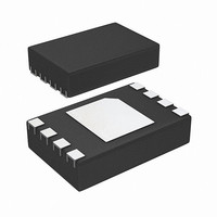
IC MEMORY MOD TEMP SENSOR 8-TDF
Manufacturer
STMicroelectronics
Specifications of STTS2002B2DN3F
Function
Temp Monitoring System (Sensor)
Topology
ADC (Sigma Delta), EEPROM, Register Bank
Sensor Type
Internal
Sensing Temperature
-40°C ~ 125°C
Output Type
I²C™/SMBus™
Output Alarm
Yes
Output Fan
No
Voltage - Supply
2.3 V ~ 3.6 V
Operating Temperature
-40°C ~ 125°C
Mounting Type
Surface Mount
Package / Case
8-TDFN
Lead Free Status / RoHS Status
Lead free / RoHS Compliant
Other names
497-10634-2
Available stocks
Company
Part Number
Manufacturer
Quantity
Price


SPD EEPROM operation
5.4.1
5.4.2
5.5
30/50
SWP and CWP
If the software write-protection has been set with the SWP instruction, it can be cleared
again with a CWP instruction.
The two instructions (SWP and CWP) have the same format as a byte write instruction, but
with a different device type identifier (as shown in
is followed by an address byte and a data byte, but in this case the contents are all “Don’t
Care”
and specific logical levels must be applied on the other two address pins A1 and A2 (as
shown in
PSWP
If the software write-protection has been set with the PSWP instruction, the first 128 bytes of
the memory are permanently write-protected. This write-protection cannot be cleared by any
instruction, or by power-cycling the device. Also, once the PSWP instruction has been
successfully executed, the SPD EEPROM no longer acknowledges any instruction (with a
device type identifier of 0110) to access the write-protection settings.
Figure 11. Setting the write protection
Write operations
Following a start condition the bus master sends a device select code with the R/W bit reset
to 0. The device acknowledges this, as shown in
The device responds to the address byte with an acknowledge bit, and then waits for the
data byte.
When the bus master generates a stop condition immediately after the ACK bit (in the “10
bit” time slot), either at the end of a byte write or a page write, the internal memory write
cycle is triggered. A stop condition at any other time slot does not trigger the internal write
cycle.
During the internal write cycle, serial data (SDA) and serial clock (SCL) are ignored, and the
device does not respond to any requests.
(Figure
Table
BUS ACTIVITY
MASTER
SDA LINE
BUS ACTIVITY
11). Another difference is that the voltage, V
20).
Doc ID 13448 Rev 8
CONTROL
BYTE
ACK
(DON'T CARE)
ADDRESS
WORD
VALUE
Figure
Table
ACK
20). Like the byte write instruction, it
12, and waits for an address byte.
(DON'T CARE)
HV
, must be applied on the A0 pin,
VALUE
DATA
ACK
STTS424E02
AI01935b
th
Related parts for STTS2002B2DN3F
Image
Part Number
Description
Manufacturer
Datasheet
Request
R

Part Number:
Description:
2.3 V memory module temperature sensor
Manufacturer:
STMicroelectronics
Datasheet:
Part Number:
Description:
STMicroelectronics [RIPPLE-CARRY BINARY COUNTER/DIVIDERS]
Manufacturer:
STMicroelectronics
Datasheet:
Part Number:
Description:
STMicroelectronics [LIQUID-CRYSTAL DISPLAY DRIVERS]
Manufacturer:
STMicroelectronics
Datasheet:

Part Number:
Description:
BOARD EVAL FOR MEMS SENSORS
Manufacturer:
STMicroelectronics
Datasheet:
Part Number:
Description:
NPN TRANSISTOR POWER MODULE
Manufacturer:
STMicroelectronics
Datasheet:
Part Number:
Description:
TURBOSWITCH ULTRA-FAST HIGH VOLTAGE DIODE
Manufacturer:
STMicroelectronics
Datasheet:
Part Number:
Description:
Manufacturer:
STMicroelectronics
Datasheet:
Part Number:
Description:
DIODE / SCR MODULE
Manufacturer:
STMicroelectronics
Datasheet:
Part Number:
Description:
DIODE / SCR MODULE
Manufacturer:
STMicroelectronics
Datasheet:
Part Number:
Description:
Search -----> STE16N100
Manufacturer:
STMicroelectronics
Datasheet:
Part Number:
Description:
Search ---> STE53NA50
Manufacturer:
STMicroelectronics
Datasheet:
Part Number:
Description:
NPN Transistor Power Module
Manufacturer:
STMicroelectronics
Datasheet: