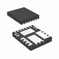
IR3831WMTR1PBF International Rectifier, IR3831WMTR1PBF Datasheet - Page 17

IR3831WMTR1PBF
Manufacturer Part Number
IR3831WMTR1PBF
Description
IC REG SYNC BUCK 8A 15-QFN
Manufacturer
International Rectifier
Series
SupIRBuck™r
Datasheet
1.IR3831WMTR1PBF.pdf
(32 pages)
Specifications of IR3831WMTR1PBF
Applications
Converter, DDR
Voltage - Input
1.5 ~ 16 V
Number Of Outputs
1
Voltage - Output
0.6 ~ 14.4 V
Operating Temperature
-40°C ~ 125°C
Mounting Type
Surface Mount
Package / Case
15-PowerVQFN
Part Status
Preferred
Package
PQFN / 5 x 6
Circuit
Single Output
Iout (a)
8
Switch Freq (khz)
250 - 1500
Input Range (v)
1.5 - 16
Output Range (v)
0.7 - 0.9*Vin
Ocp Otp Uvlo Pre-bias Soft Start And
PGOOD + EN + OVD + DDR Tracking
Server Storage
Yes
Routers Switches
Yes
Base Station Telecom
Yes
Lead Free Status / RoHS Status
Lead free / RoHS Compliant
Other names
IR3831WMTR1PBFTR
Application Information
Design Example:
The following example is a typical application for
IR3831W. The application circuit is shown on
page 22.
Enabling the IR3831W
As explained earlier, the precise threshold of
the Enable lends itself well to implementation of
a UVLO for the Bus Voltage.
For a typical Enable threshold of V
For a V
a good choice.
Programming the frequency
For F
Table. 1.
Output Voltage Programming
Output voltage is programmed by the tracking
reference voltage at Vp and external voltage
divider. The divider is ratioed such that the
voltage at the Fb pin is equal to the voltage at the
Vp pin pin when the output is at its desired value.
The output voltage is defined by using the
following equation:
Rev 14.0
V
V
R
in
o
s
2
(min)
=
in (min)
= 400 kHz, select R
=
V
R
p
V
V
I
F
*
ΔV
1
o
∗
in
o
s
R
V
=10.2V, R
⎛
⎜
⎜
⎝
=
IR3831W
=
o
=
1
1
in(
=
R
8
+
+
0.75
≤
400
Enable
12
min
A
2
R
R
R
V
22.5mV
8
9
V
EN
2
)
kHz
⎞
⎟
⎟
⎠
V
−
(
=
13.2V
V
..........
V
1
EN
=49.9K and R
EN
..........
=
max)
..........
t
1.2
= 35.7 kΩ, using
..........
(6)
EN
..........
V
= 1.2 V
in
2
R
R
=7.5kΩ is
(5)
.....(7)
1
2
When an external resistor divider is connected to
the output as shown in figure 10.
Equation (5) can be rewritten as:
For low voltage applications, such as this
design, it is often advisable to eliminate the bias
resistor R9 from Fb to ground. For the calculated
value of R8 see feedback compensation section.
Further, the tracking reference Vp may be itself
derived from some master reference by means
of a resistive divider as shown in Fig. 9. This is
common in active bus termination circuits such
as Voltage Tracking Termination (VTT) where
the tracking reference Vp may be obtained as
half of the master reference VDDQ which forms
the input to one or more memory banks.
In this design,
VDDQ=1.5V
R
Vp=0.75V
It is desirable to use a small capacitor such as
10nF in parallel with R
frequency noise on Vp pin.
Soft-Start Programming
The soft-start timing can be programmed by
selecting the soft-start capacitance value. From
(1), for a desired start-up time of the converter,
the soft start capacitor can be calculated by
using:
Where T
For tracking applications the output is generally
required to track Vp even at start-up. Hence, it is
necessary to ensure that the SS pin is already
up to 3 V before the tracking reference signal is
applied to the Vp pin. This can be done by
choosing a small value for the soft-start
capacitor to ensure that the voltage at the SS pin
rises to 3 V quickly. A 0.022 uF capacitor is
chosen for this purpose.
Fig. 10. Typical application of the IR3831W for
p1
=R
R
9
C
p2
R
R
=
SS
VDDQ
p1
p2
=1.5 kΩ
start
R
(
8
μF
programming the output voltage
∗
is the desired start-up time (ms).
⎛
⎜
⎜
⎝
)
V
=
V
o
T
−
p
Vp
V
start
IR3831WMPbF
p
IR3831W
⎞
⎟
⎟
⎠
(
..........
ms
)
p2
×
..........
Fb
0.02857
to bypass high
..........
V
..........
o
....
R8
R9
(8)
(9)
17


