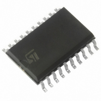
L4952D STMicroelectronics, L4952D Datasheet - Page 5

L4952D
Manufacturer Part Number
L4952D
Description
IC VREG CAR RADIO APP SO-20
Manufacturer
STMicroelectronics
Datasheet
1.L4952D.pdf
(8 pages)
Specifications of L4952D
Applications
Converter, Car Audio System
Voltage - Input
9.5 ~ 28 V
Number Of Outputs
3
Voltage - Output
8.6V, 10V
Operating Temperature
-40°C ~ 150°C
Mounting Type
Surface Mount
Package / Case
20-SOIC (7.5mm Width)
Polarity
Positive
Output Type
Fixed
Output Voltage
8.6 V, - 0.3 V to 12 V, - 0.3 V to 12 V, 10 V
Output Current
100 mA
Load Regulation
60 mV
Dropout Voltage (max)
0.5 V
Input Voltage Max
18 V
Maximum Operating Temperature
+ 150 C
Minimum Operating Temperature
- 40 C
Maximum Power Dissipation
1000 mW
Mounting Style
SMD/SMT
Voltage Regulation Accuracy
0.2 %
Lead Free Status / RoHS Status
Lead free / RoHS Compliant
Available stocks
Company
Part Number
Manufacturer
Quantity
Price
Typical Characteristics (Note 4)
is High the device is switched on. The diagnostic
circuitry detect the low drop voltage.
In this case the DIAG output is going low and can
mute the power output stage to avoid noise on
the loudspeaker.The two internal switches can
switch the stabilized output voltage with P-MOS
Transistors to one of the outputs 2 and 3 with low
drop. This is useful to switch the AM and FM cir-
cuitry on or off.
To control it there are two digital inputs En
one for each switch. EN
Low active. It’s possible to drive the AM/FM switch
with one digital line (EN
The driver for the external High side switch can
switch on and off the external pnp transistor. The
drop detection circuitry avoid the damage of the
external power pnp transistor.
To supply the varicaps and the PLL-opamp of the
car radio a second very low drop 10 V regulator is
available. This regulator in dropout has a typical
resistance of 50 .
Figure 3: Stand by consumption versus
Supply voltage rejection (C = 10 F, ESR = 4.7 ,
Load at OUT4 = 10k )
Figure 5: Supply rejection versus Frequency.
temperature
2
2
and EN
is High active and EN
3
together).
2
and En
3
is
3
Function of the external High side switch
driver
Fig 2 shows the principle circuitry of the external
High side switch. Fig. 3 shows the switch on/off
phase of the external High side switch. At the
time t0 the microcontroller switches on (curve 1 =
output signal of the microcontroller).
The signal on the HSON pin of the L4952 is shown
on curve 2. At t1 the external Power pnp is
switched on. At t2 (V
comparator compares the drop of the external pnp.
In case of normal operation the drop is smaller than
V
In case of failure (that mean a higher drop than
V
(curve 4). If an error is detected it will be stored in
the internal error flip-flop. The external pnp can
only be switched on again after having turned
HSON off (V
Figure 4: Logic input currents versus input
OUT2 propagation delay (Load = 100 )
Figure 6: OUT2 propagation delay (Load = 100 )
Dth
Dth
and no failure will be detected (curve 3).
) the external power pnp will be switched off
voltage
HSON
< V
SON1
HSON
) again.
= V
SON2
) the internal
L4952
5/8


