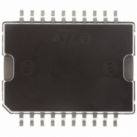
LNBP20PD STMicroelectronics, LNBP20PD Datasheet

LNBP20PD
Specifications of LNBP20PD
LNBP20PD
Available stocks
Related parts for LNBP20PD
LNBP20PD Summary of contents
Page 1
... In this occurrence the device will limit (max) the backward current that could flow from LNBA and LNBB output pins to GND. (See continuous description). Package PowerSO-20 LNBP20PD-TR Rev PowerSO-10 PowerSO-10 LNBP10SP-TR LNBP11SP-TR ...
Page 2
Contents 1 Description (continued ...
Page 3
Description (continued) For slave operation in single dish, dual receiver systems, the bypass function is implemented by an electronic switch between the Master Input pin (MI) and the LNBA pin, thus leaving all LNB powering and control functions to ...
Page 4
Pin configuration Figure 1. Pin connections (top view) PowerSO-20 Table 1. Pin Description SYMBOL NAME 15V to 25V supply Supply input V automatically selected CC1 1 when V 22V to 25V supply Supply input V ...
Page 5
Table 1. Pin Description SYMBOL NAME 22KHz tone Logic control input: see ENT enable truth table Timing capacitor used by the dynamic overload External CEXT protection. Typical capacitor application is 4.7μF for a 1200ms cycle External modulation input. Needs DC ...
Page 6
Maximum ratings Table 2. Absolute maximum ratings Symbol V DC Input voltage (V I CC1 V Output voltage O I Output current (LNBA, LNBB Logic input voltage (ENT, EN OSEL, VSEL, LLC Bypass switch current ...
Page 7
Diagram Figure 2. Block diagram 7/24 ...
Page 8
Electrical characteristics Table 5. Electrical characteristics for LNBP Series (T EN=H, ENT=L, LLC=L, V Symbol Parameter V V Supply voltage IN1 CC1 V V Supply voltage IN2 CC2 V Output voltage O1 V Output voltage O2 ΔV Line regulation ...
Page 9
Table 5. Electrical characteristics for LNBP Series (T EN=H, ENT=L, LLC=L, V Symbol Parameter Control input pin logic V IH HIGH I Control pins input current IH I Supply current CC I Output backward current OBK Temperature shutdown T SHDN ...
Page 10
Typical characteristics (unless otherwise specified T Figure 3. Output voltage vs output current Figure 5. Tone fall time vs temperature Figure 7. Tone rise time vs temperature 10/24 = 25°C) J Figure 4. Tone duty cycle vs temperature Figure ...
Page 11
Figure 9. S.V.R. vs Frequency Figure 11. Bypass switch drop vs output current Figure 13. Bypass switch drop vs output current Figure 10. External modulation vs temperature Figure 12. LNBA External modulation gain vs frequency Figure 14. Overload flag pin ...
Page 12
Figure 15. Supply voltage vs temperature Figure 17. Dynamic overload protection (I vs time) Figure 19. Tone disable 12/24 Figure 16. Supply voltage vs temperature Figure 18. Tone enable SC Figure 20. 22KHz Tone ...
Page 13
Figure 21. Enable time Figure 23. 18V to 13V Change Figure 22. Disable time Figure 24. 18V to 13V Change 13/24 ...
Page 14
Typical application schematics Figure 25. Two antenna ports receiver MCU+V 10uF C2 AUX DATA R1 47K Vcc I/Os Figure 26. Single antenna receiver with master receiver port MCU+V 10uF C2 11 AUX DATA R1 47K 13 12 Vcc I/Os ...
Page 15
Figure 27. Using serial bus to save MPU I/os MCU+V R1 AUX DATA 47K 1 4 STR CLK ...
Page 16
Figure 29. Connecting together V 4 VSEL 7 ENT OSEL LNBP10SP MCU+V Vcc I/Os Figure 30. Single antenna receiver with master receiver port - low cost solution C2 9 AUX DATA EXTM 10µF 4 VSEL 7 ENT ...
Page 17
Figure 31. Single antenna receiver with overload diagnostic MCU+V C2 AUX DATA 10µF R1 47K Vcc I/Os 17V 9 1 EXTM VCC1 2 VCC2 3 LNBA 10 OLF 8 4 CEXT VSEL 7 ENT 4.7µ ...
Page 18
Package mechanical data In order to meet environmental requirements, ST offers these devices in ECOPACK packages. These packages have a Lead-free second level interconnect. The category of second Level Interconnect is marked on the package and on the inner ...
Page 19
PowerSO-20 MECHANICAL DATA DIM. MIN 0. 0.40 c 0.23 D (1) 15.80 E 13. (1) 10 0° T (1) ...
Page 20
DIM. MIN 3.40 A3 1.25 b 0.40 c 0.35 D 9.40 D1 7.40 E 13.80 E1 9.30 E2 7. 0.95 α 0° 20/24 PowerSO-10 MECHANICAL DATA mm. TYP MAX. 3.70 0.10 3.60 1.35 ...
Page 21
Tape & Reel PowerSO-20 MECHANICAL DATA mm. DIM. MIN. TYP A C 12 15.1 Bo 16.5 Ko 3.8 Po 3.9 P 23.9 W 23.7 inch MAX. MIN. TYP. 330 13.2 0.504 0.795 2.362 30.4 ...
Page 22
Tape & Reel PowerSO10 MECHANICAL DATA DIM. MIN 12 14.9 Bo 9.9 Ko 4.15 Po 3.9 P 23.9 W 23.7 22/24 mm. TYP MAX. MIN. 330 13.2 0.504 0.795 2.362 30.4 15.1 ...
Page 23
Revision history Table 6. Revision history Date Revision 08-Jun-2004 7 21-Dec-2004 8 07-Sep-2006 9 03-May-2007 10 Changes Typing Error V and V on Table 6 - Page Table 2 has been updated on GND row. Add ...
Page 24
... Information in this document is provided solely in connection with ST products. STMicroelectronics NV and its subsidiaries (“ST”) reserve the right to make changes, corrections, modifications or improvements, to this document, and the products and services described herein at any time, without notice. All ST products are sold pursuant to ST’s terms and conditions of sale. ...


