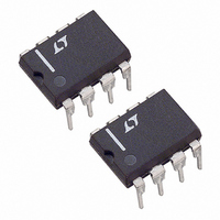
LTC1174HVCN8 Linear Technology, LTC1174HVCN8 Datasheet - Page 11

LTC1174HVCN8
Manufacturer Part Number
LTC1174HVCN8
Description
IC DC/DC CONV STP-DWN&INVRT 8DIP
Manufacturer
Linear Technology
Type
Step-Down (Buck), Invertingr
Datasheet
1.LTC1174CN8PBF.pdf
(20 pages)
Specifications of LTC1174HVCN8
Internal Switch(s)
Yes
Synchronous Rectifier
No
Number Of Outputs
1
Voltage - Output
1.25 ~ 18 V
Current - Output
1A
Frequency - Switching
200kHz
Voltage - Input
4 ~ 18.5 V
Operating Temperature
0°C ~ 70°C
Mounting Type
Through Hole
Package / Case
8-DIP (0.300", 7.62mm)
Lead Free Status / RoHS Status
Contains lead / RoHS non-compliant
Power - Output
-
Available stocks
Company
Part Number
Manufacturer
Quantity
Price
Company:
Part Number:
LTC1174HVCN8
Manufacturer:
LT
Quantity:
5 510
Company:
Part Number:
LTC1174HVCN8
Manufacturer:
LT
Quantity:
5 510
Part Number:
LTC1174HVCN8
Manufacturer:
LT
Quantity:
20 000
Company:
Part Number:
LTC1174HVCN8-3.3
Manufacturer:
LT
Quantity:
76
Part Number:
LTC1174HVCN8-3.3
Manufacturer:
LINEAR/凌特
Quantity:
20 000
Company:
Part Number:
LTC1174HVCN8-5
Manufacturer:
LT
Quantity:
200
APPLICATIO S I FOR ATIO
Board Layout Checklist
When laying out the printed circuit board, the following
checklist should be used to ensure proper operation of the
LTC1174. These items are also illustrated graphically in
the layout diagram in Figure 7. Check the following in your
layout:
1. Is the Schottky catch diode closely connected between
2. Is the “+” plate of C
3. Is the 0.1µF V
4. Is the SHUTDOWN (Pin 8) actively pulled to V
5. Is the I
ground (Pin 4) and switch (Pin 5)?
This capacitor provides the AC current to the internal
P-channel MOSFET.
between V
carries the high frequency peak currents.
normal operation? The SHUTDOWN pin is high imped-
ance and must not be allowed to float.
I
to float.
PGM
pin is high impedance and must not be allowed
PGM
IN
(Pin 7) pulled either to V
(Pin 6) and ground (Pin 4)? This capacitor
IN
decoupling capacitor closely conected
U
IN
OUTPUT DIVIDER
REQUIRED WITH
closely connected to V
VERSION ONLY
U
ADJUSTABLE
Figure 7. LTC1174 Layout Diagram (See Board Layout Checklist)
W
R2
IN
or ground? The
IN
U
R1
IN
(Pin 6)?
during
1
2
3
4
V
(V
GND
LB
LB
OUT
BOLD LINES INDICATE
FB
HIGH CURRENT PATH
OUT
IN
)
LTC1174
DESIGN EXAMPLE
As a design example, assume V
5V, and I
for this application, with I
minmum value of L is determined by assuming the
LTC1174-5 is operating in continuous mode.
With I
0.1A.The peak-to-peak ripple inductor current, I
0.5A and is also equal to:
SHUTDOWN
I
RIPPLE
I
PGM
SW
OUT
V
IN
LTC1174-3.3/LTC1174-5
OUT
8
7
6
5
= 350mA and I
=
Figure 8. Continuous Inductor Current
= 350mA maximum. The LTC1174-5 is used
4 10
D
0.1µF
•
−
6
+
⎛
⎜
⎝
TIME
C
V
C
OUT
IN
OUT
PGM
+
PEAK
L
1174 F07
+
L
(Pin 7) connected to V
V
V
V
= 0.6A (I
IN
IN
OUT
D
⎞
⎟
⎠
= 9V (nominal), V
I
AVG CURRENT = I
I
PEAK
V
(
A
LTC1174
PGM
P P
−
)
= V
=
= 350mA
I
RIPPLE
OUT
PEAK
IN
11
IN
2
), I
1174 F08
OUT
+ I
. The
1174fe
V
V
, is
=
=


