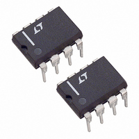
LTC1174HVCN8 Linear Technology, LTC1174HVCN8 Datasheet - Page 9

LTC1174HVCN8
Manufacturer Part Number
LTC1174HVCN8
Description
IC DC/DC CONV STP-DWN&INVRT 8DIP
Manufacturer
Linear Technology
Type
Step-Down (Buck), Invertingr
Datasheet
1.LTC1174CN8PBF.pdf
(20 pages)
Specifications of LTC1174HVCN8
Internal Switch(s)
Yes
Synchronous Rectifier
No
Number Of Outputs
1
Voltage - Output
1.25 ~ 18 V
Current - Output
1A
Frequency - Switching
200kHz
Voltage - Input
4 ~ 18.5 V
Operating Temperature
0°C ~ 70°C
Mounting Type
Through Hole
Package / Case
8-DIP (0.300", 7.62mm)
Lead Free Status / RoHS Status
Contains lead / RoHS non-compliant
Power - Output
-
Available stocks
Company
Part Number
Manufacturer
Quantity
Price
Company:
Part Number:
LTC1174HVCN8
Manufacturer:
LT
Quantity:
5 510
Company:
Part Number:
LTC1174HVCN8
Manufacturer:
LT
Quantity:
5 510
Part Number:
LTC1174HVCN8
Manufacturer:
LT
Quantity:
20 000
Company:
Part Number:
LTC1174HVCN8-3.3
Manufacturer:
LT
Quantity:
76
Part Number:
LTC1174HVCN8-3.3
Manufacturer:
LINEAR/凌特
Quantity:
20 000
Company:
Part Number:
LTC1174HVCN8-5
Manufacturer:
LT
Quantity:
200
APPLICATIO S I FOR ATIO
Catch Diode Selection
The catch diode carries load current during the off-time. The
average diode current is therefore dependent on the
P-channel switch duty cycle. At high input voltages the
diode conducts most of the time. As V
the diode conducts only a small fraction of the time. The
most stressful condition for the diode is when the output is
short-circuited. Under this condition the diode must safely
handle I
must also be used to optimize efficiency. Schottky diodes are
a good choice for low forward drop and fast switching times.
Most LTC1174 circuits will be well served by either a 1N5818,
a MBRS140T3 or a MBR0520L Schottky diode.
Short-Circuit Protection
The LTC1174 is protected from output short by its internal
current limit. Depending on the condition of I
limit is either set to 340mA or 600mA. In addition, the off-
time of the switch is increased to allow the inductor’s
current to decay far enough to prevent any current build-up
(see Figure 2).
Low-Battery Detector
The low-battery indicator senses the input voltage through
an external resistive divider. This divided voltage connects
to the “–” input of a voltage comparator (Pin 3) which is
I
PGM
I
PGM
Figure 2. Inductor's Current with Output Shorted
= V
GND
PEAK
= 0
IN
L = 100µH
V
IN
at close to 100% duty cycle. A fast switching diode
= 13.5V
U
20µs/DIV
U
W
IN
approaches V
1174 F02
PGM
U
pin, the
OUT
LTC1174 Adjustable/Low Noise Applications
The LTC1174 develops a 1.25V reference voltage between
the feedback (Pin 1) terminal and ground (see Figure 4). By
selecting resistor R1, a constant current is caused to flow
through R1 and R2 to set the overall output voltage. The
regulated output voltage is determined by:
For most applications, a 30k resistor is suggested for R1.
To prevent stray pickup, a 100pF capacitor is suggested
across R1 located close to the LTC1174. Alternatively, a
capacitor across R2 can be used to increase the switching
frequency for low noise operation.
Inverting Applications
The LTC1174 can easily be set up for a negative output
voltage. If – 5V is desired, the LTC1174-5 is ideal for this
application as it requires the least components. Figure 5
shows the schematic for this application. Note that the
compared with a 1.25V reference voltage. With the current
going into Pin 3 being negligible, the following expression
is used for setting the trip limit:
When the LTC1174 is shut down, the low-battery detector
is inactive.
V
V
LBTRIP
OUT
LTC1174-3.3/LTC1174-5
=
1 25 1
=
.
Figure 3. Low-Battery Comparator
1 25 1
V
.
IN
⎛
⎜
⎝
⎛
⎜
⎝
+
R
R
+
2
1
R4
R3
R
R
⎞
⎟
⎠
3
4
3
⎞
⎟
⎠
–
+
LTC1174
1.25V
REFERENCE
1174 F03
LTC1174
1174fe
9


