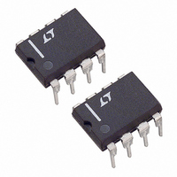
LTC1174HVCN8 Linear Technology, LTC1174HVCN8 Datasheet - Page 6

LTC1174HVCN8
Manufacturer Part Number
LTC1174HVCN8
Description
IC DC/DC CONV STP-DWN&INVRT 8DIP
Manufacturer
Linear Technology
Type
Step-Down (Buck), Invertingr
Datasheet
1.LTC1174CN8PBF.pdf
(20 pages)
Specifications of LTC1174HVCN8
Internal Switch(s)
Yes
Synchronous Rectifier
No
Number Of Outputs
1
Voltage - Output
1.25 ~ 18 V
Current - Output
1A
Frequency - Switching
200kHz
Voltage - Input
4 ~ 18.5 V
Operating Temperature
0°C ~ 70°C
Mounting Type
Through Hole
Package / Case
8-DIP (0.300", 7.62mm)
Lead Free Status / RoHS Status
Contains lead / RoHS non-compliant
Power - Output
-
Available stocks
Company
Part Number
Manufacturer
Quantity
Price
Company:
Part Number:
LTC1174HVCN8
Manufacturer:
LT
Quantity:
5 510
Company:
Part Number:
LTC1174HVCN8
Manufacturer:
LT
Quantity:
5 510
Part Number:
LTC1174HVCN8
Manufacturer:
LT
Quantity:
20 000
Company:
Part Number:
LTC1174HVCN8-3.3
Manufacturer:
LT
Quantity:
76
Part Number:
LTC1174HVCN8-3.3
Manufacturer:
LINEAR/凌特
Quantity:
20 000
Company:
Part Number:
LTC1174HVCN8-5
Manufacturer:
LT
Quantity:
200
FU CTIO AL DIAGRA
PI FU CTIO S
V
main voltage comparator’s input. On the LTC1174-3.3 and
LTC1174-5 this pin goes to an internal resistive divider
which sets the output voltage.
LB
pin will sink current when Pin 3 (LB
During shutdown the state of this pin is indeterminate.
LB
Comparator. The “+” input is connected to a reference
voltage of 1.25V.
GND (Pin 4): Ground Pin.
LTC1174
LTC1174-3.3/LTC1174-5
6
OUT
OUT
IN
U
U
g
m
(V
(Pin 3): The “–” Input of the Low-Battery Voltage
LB
V
(Pin 2): Open Drain of an N-Channel Pull-Down. This
FB
GND 4
FB
OUT
) (Pin 1): For the LTC1174, this pin connects to the
U
2
U
C
U
T
V
TH2
A3
+
–
V
TH1
–
+
–
+
W
IN
A4
A5
) goes below 1.25V.
LB
3
IN
(Pin 1 connection shown for LTC1174-3.3 and LTC1174-5, changes create LTC1174)
REFERENCE
* R1 = 51k FOR LTC1174-3.3
R1 = 93.5k FOR LTC1174-5
1.25V
SLEEP
SET
RESET
V
SHUTDOWN
6
IN
SW (Pin 5): Drain of the P-Channel MOSFET Switch. Cathode
of Schottky diode must be closely connected to this pin.
V
close to ground Pin 4.
I
Switch. With I
with I
SHUTDOWN (Pin 8): Pulling this pin to ground keeps the
internal switch off and puts the LTC1174 in micropower
shutdown.
PGM
8
IN
(Pin 6): Input Supply Voltage. It must be decoupled
Q
PGM
(Pin 7): Selects the Current Limit of the P-Channel
= 0V, the current trip value is reduced to 340mA.
A2
PGM
+
–
= V
IN
A1
V
, the current trip point is 600mA and
LIM1
–
+
V
LIM2
V
I
V
PGM
OUT
FB
7
×
1
(V
31.5k
R1*
FB
)
SW
5
R
0.1Ω
SENSE
1174 BD
1174fe


