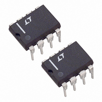
LTC1174HVCN8 Linear Technology, LTC1174HVCN8 Datasheet - Page 7

LTC1174HVCN8
Manufacturer Part Number
LTC1174HVCN8
Description
IC DC/DC CONV STP-DWN&INVRT 8DIP
Manufacturer
Linear Technology
Type
Step-Down (Buck), Invertingr
Datasheet
1.LTC1174CN8PBF.pdf
(20 pages)
Specifications of LTC1174HVCN8
Internal Switch(s)
Yes
Synchronous Rectifier
No
Number Of Outputs
1
Voltage - Output
1.25 ~ 18 V
Current - Output
1A
Frequency - Switching
200kHz
Voltage - Input
4 ~ 18.5 V
Operating Temperature
0°C ~ 70°C
Mounting Type
Through Hole
Package / Case
8-DIP (0.300", 7.62mm)
Lead Free Status / RoHS Status
Contains lead / RoHS non-compliant
Power - Output
-
Available stocks
Company
Part Number
Manufacturer
Quantity
Price
Company:
Part Number:
LTC1174HVCN8
Manufacturer:
LT
Quantity:
5 510
Company:
Part Number:
LTC1174HVCN8
Manufacturer:
LT
Quantity:
5 510
Part Number:
LTC1174HVCN8
Manufacturer:
LT
Quantity:
20 000
Company:
Part Number:
LTC1174HVCN8-3.3
Manufacturer:
LT
Quantity:
76
Part Number:
LTC1174HVCN8-3.3
Manufacturer:
LINEAR/凌特
Quantity:
20 000
Company:
Part Number:
LTC1174HVCN8-5
Manufacturer:
LT
Quantity:
200
OPERATIO
The LTC1174 uses a constant off-time architecture to
switch its internal P-channel power MOSFET. The off-time
is set by an internal timing capacitor and the operating
frequency is a function of V
The output voltage is set by an internal resistive divider
(LTC1174-3.3 and LTC1174-5) or an external divider re-
turned to V
compares the divided output voltage to a reference voltage
of 1.25V.
To optimize efficiency, the LTC1174 automatically switches
between continuous and Burst Mode
age comparator is the primary control element when the
device is in Burst Mode operation, while the current com-
parator controls the output voltage in continuous mode.
During the switch“ON” time, switch current flows through
the 0.1Ω sense resistor. When this current reaches the
threshold of the current comparator A2, its output signal will
change state, setting the flip-flop and turning the switch off.
The timing capacitor, C
voltage goes below V
which resets the flip-flop and causes the switch to turn on
again. Also, the timing capacitor is recharged. The inductor
current will again ramp up until the current comparator A2
trips. The cycle then repeats.
When the load is relatively light, the LTC1174 automatically
goes into Burst Mode operation. The current mode loop is
interrupted when the output voltage reaches the desired
regulated value. The hysteretic voltage comparator A1 trips
when V
the switch and causing the timing capacitor to discharge.
This capacitor discharges past V
below V
generated.
OUT
TH2
. Comparator A5 then trips and a sleep signal is
is above the desired output voltage, shutting off
FB
Pin 1 (LTC1174). A voltage comparator A1
U
(Refer to Functional Diagram)
TH1
T
. Comparator A4 will then trip,
, begins to discharge until its
IN
.
TH1
until its voltage drops
®
operation. The volt-
Burst Mode is a registered trademark of Linear Technology Corporation.
In sleep mode, the LTC1174 is in standby and the load
current is supplied by the output capacitor. All unused
circuitry is shut off, reducing quiescent current from
0.45mA to 0.13mA. When the output capacitor discharges
by the amount of the hysteresis of the comparator A1, the
P-channel switch turns on again and the process repeats
itself.
Operating Frequency and Inductor
Since the LTC1174 utilizes a constant off-time architecture,
its operating frequency is dependent on the value of V
frequency of operation can be expressed as:
where t
Note that the operating frequency is a function of the input
and ouput voltage.
Although the size of the inductor does not affect the fre-
quency, it does affect the ripple current. The peak-to-peak
ripple current is given by:
By choosing a smaller inductor, a low ESR output filter
capacitor has to be used (see C
loss will also increase (see Inductor Core Selection section)
due to higher ripple current.
I
f
RIPPLE
=
t
OFF
OFF
1
LTC1174-3.3/LTC1174-5
= 4µs and V
=
⎛
⎜
⎝
4 10
V
IN
V
•
IN
−
+
−
V
6
OUT
V
D
⎛
⎜
⎝
D
is the voltage drop across the diode.
V
OUT
⎞
⎟
⎠
L
+
( )
IN
Hz
V
and C
D
⎞
⎟
⎠
OUT
(
A
LTC1174
). Moreover, core
P P
−
)
IN
. The
1174fe
7


